.
XV-CIE
1
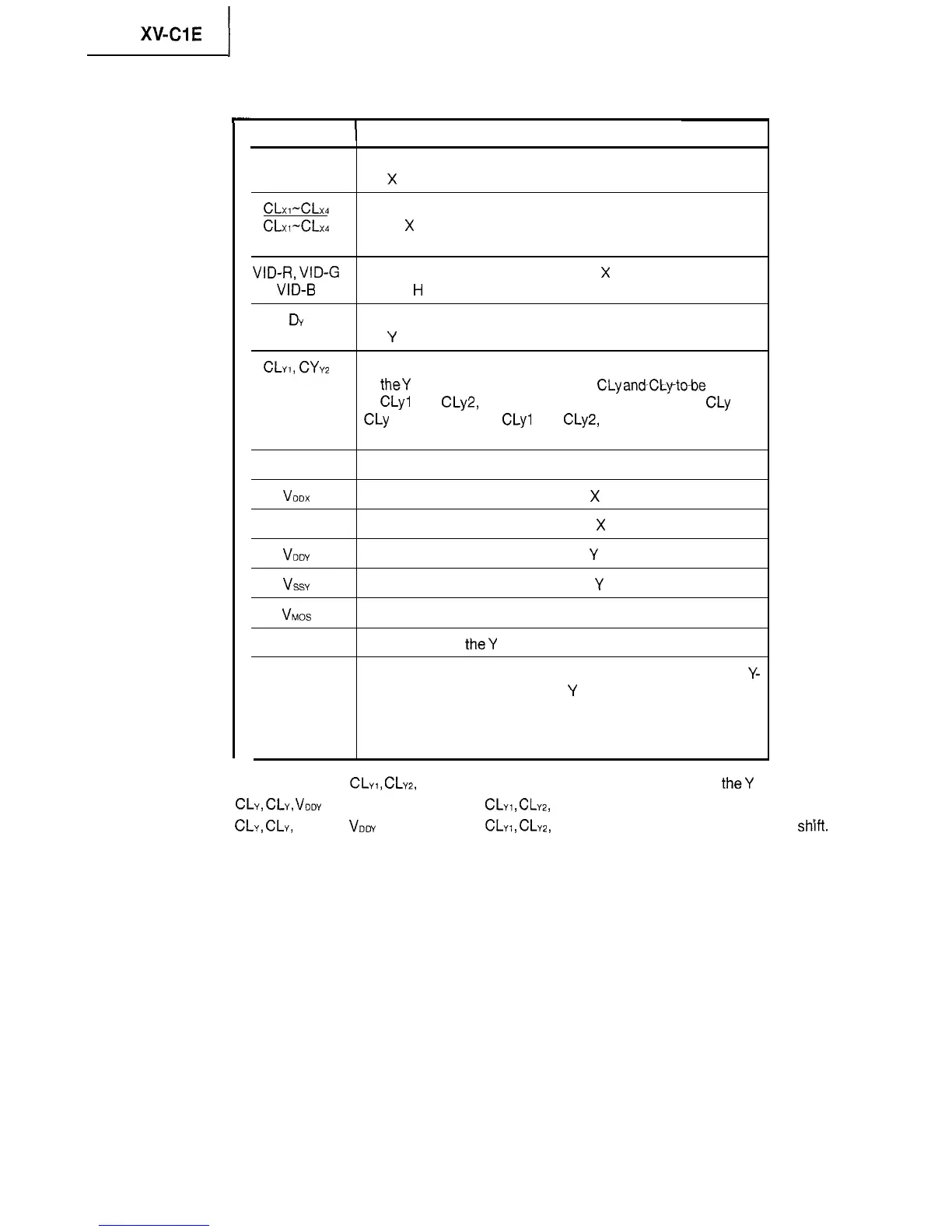
II. Input terminals
-
Pin name
I
Function
Dx
Used to input a start pulse for the X-shift register (component of
the
X
driver).
CLx,-CLXd
CLxt-CLx4
Used to input a transfer clock for the X-shift register (component
of the
X
driver). Composed of 4 clocks (45” shifted from each
other) and their 4 inverted signals.
VID-R,
VID-G
Used to input the video signal for the
X
driver. Polarity inverted
VID-B every 1
H
period.
DY
Used to input a start pulse for the Y-shift register (component of
the
Y
driver).
CLYI,
CYY2
Used to input
a
transfer clock for the Y-shift register (component
of
they
driver) and its inverted signal.
CLy
and-CLy-to-be
inputted
to CLyl and
CLy2,
respectively, for forward shift, and
CLy
and
CLy
to be inputted to CLyl and
CLy2,
respectively, for reverse
shift.
LCCOM
voox
vssx
VDDY
VSSY
VMOS
ENABLE
DIR, DIR
Used to input a counter-electrode potential of the LCD panel.
Used to input positive power for the
X
driver.
Used to input negative power for the
X
driver.
Used to input positive power for the
Y
driver.
Used to input negative power for the
Y
driver.
Used to input a common potential for the holding capacitor.
Used to enable
they
driver output.
Used to input the signal for switching the shift direction of the
Y-
shift register (component of the
Y
driver). Vddy and Vssy to be
inputted to DIR and DIR, respectively, for forward shift, and Vssy
and Vddy to be inputted to DIR and DIR, respectively, for re-
verse shift.
Note 1:
Inputs to be made to
CLYI,
CLYZ,
DIR, and DIR for switching the shift direction of
they
driver.
(1)
CLY,
CLY,
VODY
and
V
SSY
to be inputted to
CLYI,
CLYZ,
DIR and DIR, respectively, for forward shift.
(2)
CLY,
CLY,
V
SSY
and
VODY
to be inputted to
CLY~,
CLYZ,
DIR and DIR, respectively, for reverse
shift.
36