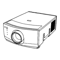
xv-zw99u
DESCRIPTION OF
SCHEMATIC DIAGRAM
VOLTAGE MEASUREMENT CONDITION:
1. Voltages at test points are measured at the
supply voltage of AC 120V. Signals are fed by a
color bar signal generator for servicing purpose and
the above voltages are measured with a 20k ohm/V
tester,
WAVEFORM MEASUREMENT CONDI-
TION:
1. Waveforms at test points are observed at the supply
voltage of AC 12OV. Signals are fed by a color bar
signal generator for servicing purpose.
INDICATION OF RESISTOR & CAPACI-
TOR:
RESISTOR
1. The unit of resistance “Q” is omitted.
(K=kR=lOOO R, M=MQ).
2. All resistors are f 5%, unless otherwise noted.
(J= zt 5%, F= zt l%, D= zt 0.5%)
3. All resistors are l/l OW, unless otherwise noted.
4. All resistors are Carbon type, unless otherwise
noted.
0: Solid 8: Cement
0: Oxide Film
0: Special
0: Metal Coating
CAPACITOR
1. All capacitors are uF, unless otherwise noted.
(P=pF=uuF).
2. All capacitors are 5OV, unless otherwise noted.
3. All capacitors are Ceramic type, unless otherwise
noted.
(ML): Mylar
(TA): Tantalum
(PF): Polypro Film (ST): Styrol
CAUTION:
This circuit diagram is original one, therefore there may be a
slight difference from yours.
SAFETY NOTES:
1. DISCONNECT THE AC PLUG FROM THE AC
OUTLET BEFORE REPLACEING PARTS.
2. SEMICONDUCTOR HEAT SINKS SHOULD BE
REGARDED AS POTENTIAL SHOCK HAZARDS
WHEN THE CHASSIS IS OPERATING.
IMPORTANT SAFETY NOTICE:
PARTS MARKED WITH “A (
) ARE
IMPORTANT FOR MAINTAINING THE SAFETY OF
THE SET. BE SURE TO REPLACE THESE PARTS
WITH SPECIFIED ONES FOR MAINTAINING THE
SAFENAND PERFORMANCE OF THE SET.
46

 Loading...