8.4.7 LVCMOS Output Polarity
When a driver is configured as an LVCMOS output it generates a clock signal on both pins (OUTx and OUTxb). By default the clock
on the OUTx pin is generated with the same polarity (in phase) with the clock on the OUTxb pin. The polarity of these clocks is
configurable enabling complimentary clock generation and/or inverted polarity with respect to other output drivers.
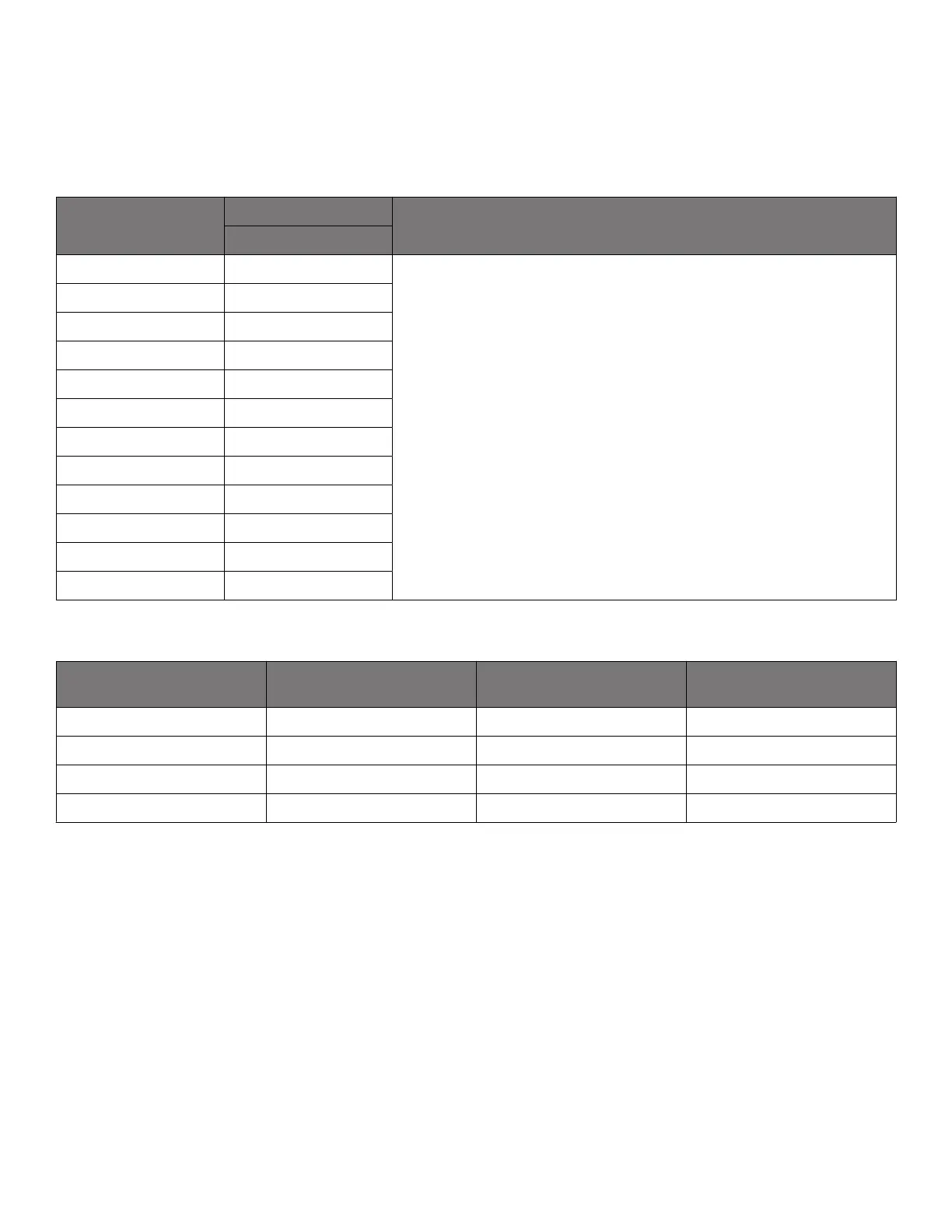
Table 8.8. LVCMOS Output Polarity Control Registers
Setting Name Hex Address [Bit Field] Function
Si5391 only
OUT0A_INV 0106[7:6] Controls output polarity of the OUTx and OUTxb pins when in LVCMOS mode.
Selections are as below in the Output Polarity Registers.
OUT0_INV 010B[7:6]
OUT1_INV 0110[7:6]
OUT2_INV 0115[7:6]
OUT3_INV 011A[7:6]
OUT4_INV 011F[7:6]
OUT5_INV 0124[7:6]
OUT6_INV 0129[7:6]
OUT7_INV 012E[7:6]
OUT8_INV 0133[7:6]
OUT9_INV 0138[7:6]
OUT9A_INV 013D[7:6]
Table 8.9. Output Polarity of OUTx and OUTxb Pins in LVCMOS Mode
OUTx_INV
Register Settings
OUTx OUTxb Comment
00 CLK CLK Both in phase (default)
01 CLK CLKb OUTxb inverted
10 CLKb CLKb OUTx and OUTxb inverted
11 CLKb CLK OUTx inverted
Si5391 Reference Manual • Outputs
Skyworks Solutions, Inc. • Phone [781] 376-3000 • Fax [781] 376-3100 • sales@skyworksinc.com • www.skyworksinc.com
33 Rev. 0.5 • Skyworks Proprietary Information • Products and Product Information are Subject to Change Without Notice • January 11, 2022 33
 Loading...