4-2 (E)
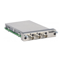
BKM-21D
. .
. .
. In case of the D2 PAL signal
The 10-bit parallel signal output from IC95 to IC100 is
separated from its audio signal by IC120 to become the
digital composite video signal. This signal is D/A convert-
ed by IC128 to become the INT V signal, level-adjusted by
IC300, bandwidth-limited by LPF (FL301), and the sync-
tip clamped to 2 V by Q322 to Q324. At that time, the 100
IRE level corresponds to approximately 3.5 V. This signal
is input to the A/D converter (IC341), converted to the 10-
bit parallel data (B-Y sampling phase), Y/C separated, and
input to the decoder circuit (IC303 to IC306, and IC309).
The 10-bit parallel signal is passed through IC303 and
IC304 to become 2H delay signal. It is then passed through
IC305 and IC306 to become the 4H delay signal. These 2H
delay signal, 4H delay signal, and no-delay signal (0H
signal) are input to IC309, Y/C separated in the Y/C
separated filter inside IC309 to become the Y signal and
chroma signal. The Y signal is output as it is, while the
chroma signal is decoded to the R-Y and B-Y signals to
output.
The Y signal output from IC309 is input to IC318 (Y
signal delay) directly. The B-Y and R-Y signals are passed
through the PAL-S process circuit (IC361 and IC360) in
the PAL-S mode, or through the PAL-D process circuit
(IC903, IC904, and IC908 to IC919) in the PAL-D mode,
and input to IC319 (B-Y signal delay) and IC320 (R-Y
signal delay). The three signals which pass through the
delay circuit are input to the D/A converter (IC370), and
converted to the analog signals (Y signal, B-Y signal, and
R-Y signal).
4-1-3. Low Pass Filter, Amplifier Circuit
4-1-3-1.Y signal
The Y signal output from the D/A converter (IC370) is
bandwidth-limited by the LPF (FL701), passed through the
amplifier circuit (Q712 and 737), switching circuit (Q738,
739, 760, 761), and output to the aperture compensation
circuit (Q408, IC501) of the analog signal system.
4-1-3-2.B-Y Signal, R-Y Signal
The B-Y signal that is output from the D/A converter
(IC370) is bandwidth-limited by LPF (FL703) passed
through the amplifier circuit (Q719 and Q720) and switch-
ing circuit (Q721 to Q724), and finally output to the level
adjustment circuit (IC601) of the analog signal system.
This is the same for the R-Y signal.
4-1-4. EXTERNAL-DIGITAL Input Circuit
The BKM-21D is able to carry out external parallel digital
input via the BKM-20D and BKM-22X. External digital
signals are input to the bi-directional buffers (IC125 and
IC126) via FB110 to FB120 from CN3. The signal output
from this IC is interrupted into the IC95 to IC100 output
bus lines, and input to IC115 or IC120.
4-1-5. DIGITAL FORMAT Detection Circuit
Pin 2 (SYNC terminal) of the SDI decoder (IC101,
IC104, and IC106) outputs the pulse that inverts its signal
phase whenever it detects the TRS (Timing Reference
Signal) in the input data when it receives the correct signal.
This pulse is input to the monostable multivibrator (IC50)
and fixed at level “H” with the 10 usec time constant.
When reception errors occur, PIN 2 (SYNC terminal) of
the SDI decoder ((IC101, IC104, and IC106) does not
output any pulse. For this reason, the output of the
monostabel multivibrator (IC50) is fixed at level “L”. This
discrimination signal is sent to the CPU (IC802).
4-1-6. D2 D/A Video Signal Output Circuit
In this system, the analog signal is output to another
decoder board via video bus line after implementing D/A
conversion by IC128. In this case, the INT-V OUT signal
goes “Low” and Q414 turns ON. The INT V signal of the
D/A converter output passes through IC300, FL301, Q440,
Q441, Q444, and Q446, and is adjusted of its level by
IC401, and is output via Q413 and Q415.


 To Next Page