4-3 (E)
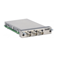
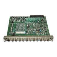
BKM-21D
4-2. Analog Signal System
4-2-1. Input Switching Circuit, Aperture
Compensation Circuit, Output Circuit
4-2-1-1.Composite Video Signal Input Switching
Circuit (Q401 to 403, 433, 501 to 503, 522,
601 to 603, 624)
When channel A is selected, the V-A signal becomes “L”,
Q402 turns ON, and the composite video signal is passed
through the buffer amplifier (Q403) and output to the A/D
converter circuit. This is the same when other channels
(channels B, C) are selected.
However, in the bypass mode, the signal is not passed
through the Y/C separation circuit, but input to the aperture
compensation circuit directly.
4-2-1-2.Y/R-Y/B-Y Signal Input Circuit (Q401, 420,
421, 434, 501, 520, 521, 523, 601, 625, 640,
641)
The YPBPR signal becomes “L”. The Y signal is passed
through Q401, 434, 420, and 421, and output to the
aperture circuit. The B-Y signal is passed through Q501,
523, 520, and 521, and output to the B-Y signal delay. This
is the same for the R-Y signal.
4-2-1-3.R/G/B Signal Input Circuit (Q401, 501, 601,
605 to 607, 611 to 614)
The RGB signal becomes “L”. The G signal is passed
through Q401, 605, and 607, and output to the level
adjustment circuit. This is the same for the B and R
signals.
4-2-1-4.Aperture Compensation Circuit (IC501,
Q408, 409, 505 to 509, 512 to 514)
The aperture compensation signal is made by the two delay
lines (DL501, 502). This compensation signal is level-
adjusted by IC501, and mixed with the Y signal. The
aperture compensation amount is controlled by the APT
voltage. The aperture-compensated Y signal is passed
through the switching circuit (Q512 to 514), and output to
the level adjustment circuit. The APT voltage is output
from the D/A converter (IC805) of the control circuit.
4-2-1-5.R-Y/B-Y Signal Delay Circuit (Q404, 418,
419, 422 to 425, 450)
In the case of the Y, R-Y, and B-Y signals input, the Y
signal is delayed by the aperture compensation circuit and
the R-Y and B-Y signals are delayed by DL402 and
DL403.
4-2-1-6. Level Adjustment Circuit, Output Circuit
(IC401, 502, 601, 602, Q413 to 415, 515 to
517, 615, 616, 619 to 623)
The Y/G signal is explained.
When signals other than the RGB signal is input, the Y
signal from the Y signal delay circuit is input to Pin 1 of
IC502, level-adjusted by IC502, and output to Pin 5. It is
then passed through the switching circuit (Q515 to 518)
and output from Pin
11B
of CN2. The gain of IC502 is
controlled by the Y LEVEL voltage input to pin 3. The
switching circuit (Q515 to 518) is controlled by the OE
signal.
When the RGB signal is input, the G signal from the RGB
signal switch (Q606, 607) is input to Pin 1 of IC502.
Hereafter, it is the same as the Y signal.
4-2-1-7.Composite Video I/O Circuit
This system is capable of transmitting and receiving the
composite video signal with other decoder boards using the
video bus line.
When the signal input from the BNC terminal of BKM-
21D is sent to other decoder boards, the INT-V OUT signal
becomes L and Q414 turns ON. The composite video
signal is level-adjusted by IC401, and output via Q413 and
Q415.
When the composite video signal is received from other
decoder boards, the EXT-V OUT signal becomes L, Q411
turns ON, and the composite signal is output to the A/D
conversion circuit via Q410 and Q412.
4-3. A/D Conversion Circuit
(IC300, IC341)
The composite video signal is level-adjusted by IC300,
bandwidth-limited by the LPF (FL301), sync-clamped to 2
V by Q322 to 324. The 100 IRE level is about 3.5 V at that
time. This signal is input to the A/D converter (IC341) and
converted to the 10-bit parallel data. Hereafter, the same
signal processing as the D2 NTSC or D2 PAL signal is
performed.
http://getMANUAL.com


 To Next Page