57
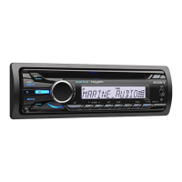
CDX-5V661/5V661A/5V661D/5V661S
4-15. IC PIN FUNCTION DESCRIPTION
• MAIN BOARD IC801 HD6432357M05F (SYSTEM CONTROLLER)
Pin No. Pin Name I/O Description
1
K3
I
Key input terminal S5, S6 (3) “L”: active
2
K4 I Key input terminal S7, S8 (4) “L”: active
3
GND — Ground terminal
4
NC — Not used (open)
5VCC
— Power supply terminal (+3.3V)
6K5I
Key input terminal S9, S10 (5) “L”: active
7
K6
I
Key input terminal S11, S12 (6) “L”: active
8
K LOAD I LOAD key input terminal S13, S14 (LOAD) “L”: active
9 K EJECT
I EJECT key input terminal S15, S16 (EJECT) “L”: active
10
GND — Ground terminal
11
SW1–6 O LED drive signal output to the front panel 1 to 6 key LEDS (1 to 6) “H”: LED on
12
SWLOAD O LED drive signal output to the front panel LOAD key (LOAD) “H”: LED on
13 SWEJECT
O LED drive signal output to the front panel EJECT key (EJECT) “H”: LED on
14 IND1
O LED drive signal output to the front panel (disc address 1) “H”: LED on
15 IND2
O LED drive signal output to the front panel (disc address 2) “H”: LED on
16 IND3
O LED drive signal output to the front panel (disc address 3) “H”: LED on
17
IND4 O LED drive signal output to the front panel (disc address 4) “H”: LED on
18 IND5
O LED drive signal output to the front panel (disc address 5) “H”: LED on
19 GND
— Ground terminal
20 IND6 O
LED drive signal output to the front panel (disc address 6) “H”: LED on
21 INDSLOT O
LED drive signal output to the front panel (disc slot) “H”: LED on
22 DSTC R I
Disc chucking end/save end detect switch input terminal (right)
(When completion of the disc chucking/save operation)
23 DSZ
I Disc size detection signal input terminal
24 DSTC L
I
Disc chucking end/save end detect switch input terminal (left)
(When completion of the disc chucking/save operation)
25
S SCL I Shutter close detect switch input terminal
26 EECKO
O Serial clock signal output to the EEPROM (IC810)
27
EESIO
I/O
Two-way serial data bus with the EEPROM (IC810)
28
GND — Ground terminal
29
POS I Optical pick-up block address detect sensor input terminal
30
HOME I Optical pick-up home position detect switch input terminal
31
SOSY I Subcode sync (SO + SI) detect signal input from the CXD3027R (IC601)
32
GRSCOR I
Subcode sync (SO + SI) detect signal input from the D-RAM controller section on the
CXD3027R (IC601)
33
OPP I Lever (op) SW (play position) detect switch input terminal “L”: Active
34
BU IN I Back-up sens input terminal “6.5V”: Voltage low detect
35
GND — Ground terminal
36
GND — Ground terminal
37
WAKEUP I Wake-up input terminal “L”: ACC on
38
KEYACK I Input of acknowledge signal for the key entry On at input of “H”
39 VDD
I Power supply terminal (+3.3V)
40
OPH I Lever (op) SW (home position) detection input terminal
41
LMT IN I Sled limit in detect switch input terminal “L”: When the optical pick-up is inner position
42
FOLOCK O Lens focus lock signal output terminal
43
R/RW SW O CD-ROM/CD-RW select signal output to the CXA2581N (IC201) “L”: RW, “H”: ROM
w
w
w
.
x
i
a
o
y
u
1
6
3
.
c
o
m
Q
Q
3
7
6
3
1
5
1
5
0
9
9
2
8
9
4
2
9
8
T
E
L
1
3
9
4
2
2
9
6
5
1
3
9
9
2
8
9
4
2
9
8
0
5
1
5
1
3
6
7
3
Q
Q
TEL 13942296513 QQ 376315150 892498299
TEL 13942296513 QQ 376315150 892498299
http://www.xiaoyu163.com
http://www.xiaoyu163.com
 Loading...