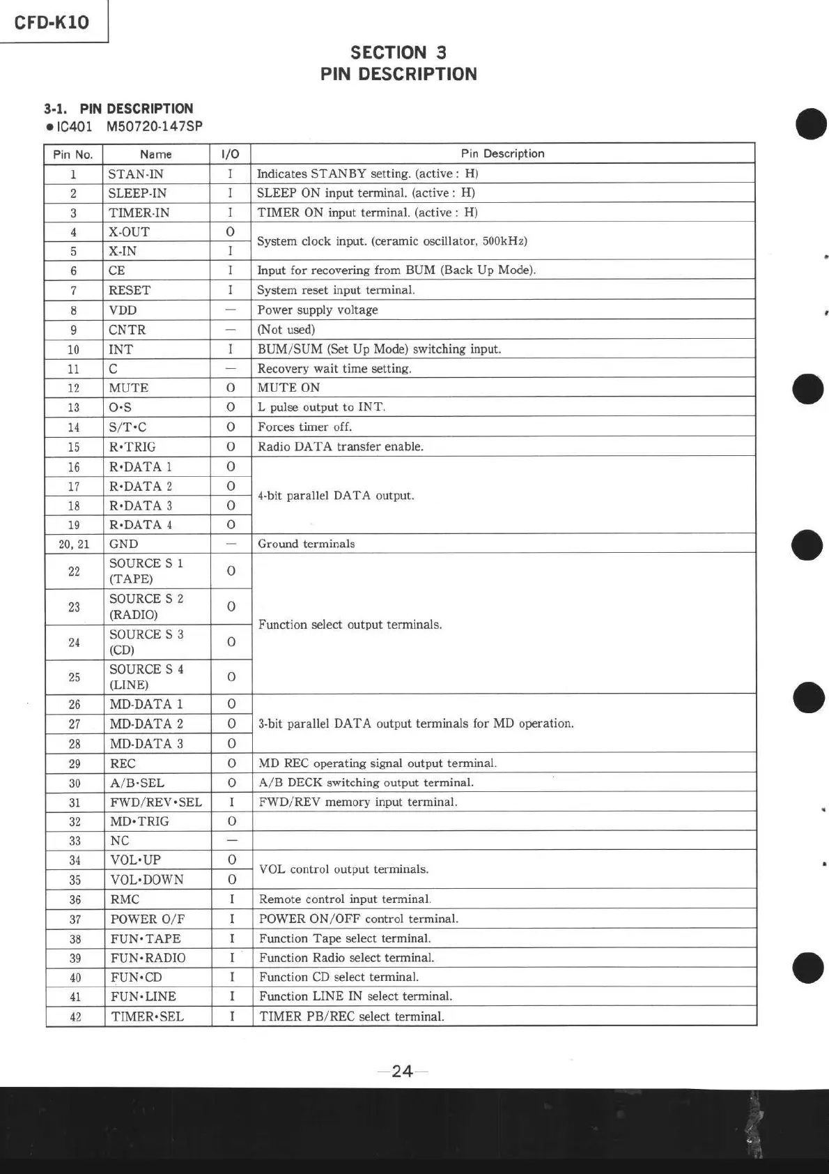
sEcTtoN 3
PIN DESCRIPTION
3.1,
PIN DESCRIPTION
.tc401
M50720-147SP
Pin No.
Name
t/o
Pin Description
I STAN.IN
I Indicates
STANBY
setting.
(active
:
H)
2 SLEEP.IN
I
SLEEP ON
input terminal.
(active
:
H)
TIMER-IN
I TIMER ON input terminal.
(active
: H)
,l
X.OUT o
System clock
input.
(ceramic
oscillator, 500kHz)
E
X.IN
I
o
CE
I Input for recovering
from BUM
(Back
Up
Mode).
7
RESET System
reset input terminal.
8 VDD
Power supply voltage
9 CNTR
(Not
used)
10 INT
I
BUM/SUM
(Set
Up Mode) switching
input.
11
Recovery wait time setting.
t2 MUTE
o MUTE ON
13
o.s
o
L
pulse
output to INT.
I4 S/T.C
o
Forces
timer off.
ta
R.TRIG
o Radio DATA transfer enable.
lo R.DATA 1 o
4-bit
parallel
DATA output.
77 R.DATA
2
18 R.DATA 3 o
19 R.DATA
4 o
20,2L GND
Ground terminals
22
SOURCE S
1
(TAPE)
o
Function select output terminals.
23
SOURCE S
2
(RADTO)
o
24
SOURCE S
3
(cD)
o
25
SOURCE
S 4
(LINE)
o
26 MD.DATA
1 o
3-bit
parallel
DATA output terminals
for MD
operation.
27
MD.DATA 2 o
28 MD.DATA 3 o
29 REC
o
MD REC
operating
signal output terminal.
30
A/B.SEL
o
A/B DECK
switching
output terminal.
31
F\A/D/REV.SEL
I FWD/REV memory
input
terminal.
32
MD.TRIG
o
aa
NC
J4l
VOL.UP
o
VOL control output terminals.
JJ vol..Do\4rN o
JO RMC
I Remote control
input
terminal.
37 POWER O/F
I
POWER
ON/OFF
control terminal.
38
FUN.TAPE
I Function Tape select terminal.
39
FUN.RADIO
Function Radio select terminal.
40
FUN.CD
I Function CD select terminal.
41 FUN.LINE
I Function
LINE IN select terminal.
TIMER.SEL
I TIMER
PB/REC
select terminal.
-24-