cFp-K1o
I
o
o
o
o
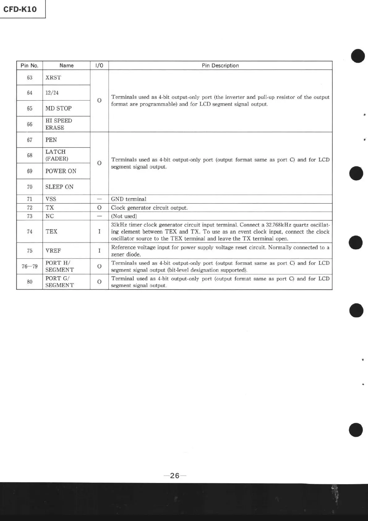
Pin No. Name t/o Pin Description
63
XRST
o
Terminals
used as
4-bit
output-only
port
(the
inverter and
pull-up
resistor of tlre output
64
12/24
OJ MD
STOP
format are
programmable)
and
for LCD
segment signal output.
66
HI SPEED
ERASE
67
PEN
o
Terminals
used as 4-bit output-only
port
(output
format same as
port
C) and for LCD
68
LATCH
(FADER)
69
POWER
ON
segment signal output.
70 SLEEP ON
tl
VSS GND terminal
72 TX o Clock
generator
circuit output.
,72
NC
(Not
used)
74 TEX
I
32kHz
timer clock
generator
circuit input terminal. Connect a 32.768kH2
quartz
oscillât-
ing element between TEX and TX. To
use
as an event clock input,
connect the clock
oscillator source to the TEX
terminal and
leave
the
TX
terminal open.
VREF I
Reference
voltage
input
for
power
supply voltage reset circuit. Normally connected
to
a
zener
diode.
76-79
PORT H/
SEGMENT
o
Terminals
used as
4-bit
output-only
port
(output
format same as
port
C) and for LCD
segment signal output
(bit-level
designation supported).
80
PORT
G/
SEGMENT
(,
Terminal
used as 4-bit
output-only
port (output
format same as
port
C) and for LCD
segment signal output.
-26-
o