47
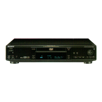
DVP-S9
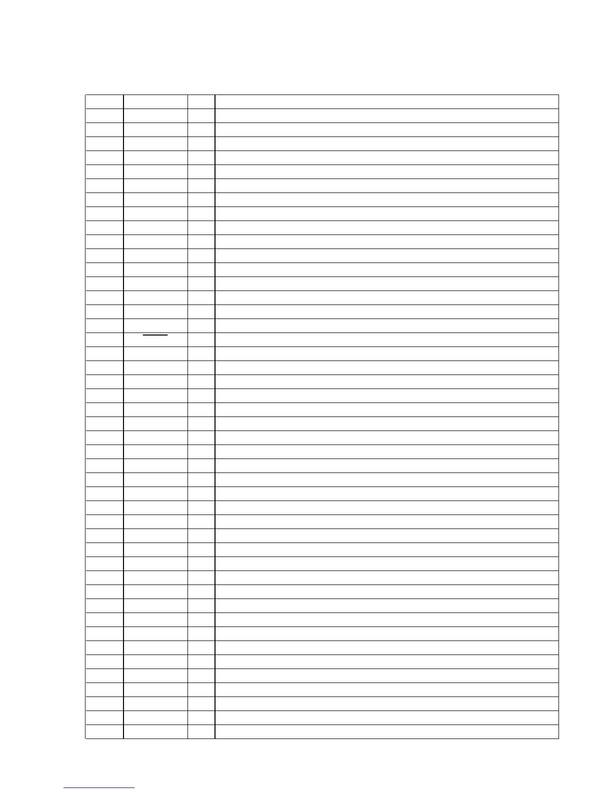
6-22. IC PIN FUNCTION DESCRIPTION
• RF BOARD IC001 SP3728AC (DVD/CD RF AMP, FOCUS/TRACKING ERROR AMP)
Pin No. Pin Name I/O Description
1, 2 RFIP, RFIN I
RF signal input terminal
3CP—
Tracking LPF terminal
4WINI
Wobble detection signal input terminal Not used (open)
5WPPO
Wobble push-pull signal output terminal Not used (open)
6CN—
Tracking LPF terminal
7 to 10 A2 to D2 I
Photo detector interface input terminal (AC coupled input for the DPD and wobble)
11 to 14 D to A I
Photo detector interface input terminal (main)
15 to 18 E to H I
Photo detector interface input terminal (sub)
19 VC O
Reference voltage (+2.5V) output terminal
20 VPB —
Power supply terminal (+5V) (servo block)
21 DVDPD I
DVD APC signal input terminal
22 CDPD I
CD APC signal input terminal
23 VNB —
Ground terminal (servo block)
24 LDSELO O
APC LD select signal output terminal
25 DVDLD O
DVD APC signal output terminal
26
CDLD O
CD APC signal output terminal
27
LDON I
APC LD output control signal input terminal
28
MEVO O
Envelope signal output terminal for mirror
29
MIN I
RF signal input terminal for mirror
30
MP —
Mirror top hold terminal
31
MB —
Mirror bottom hold terminal
32
MLPF —
Mirror LPF terminal
33
MIRR O
Mirror detect signal output to the servo DSP (IC302)
34
BYP2 —
Servo AGC gain control terminal
35
PII I
Pull-in signal input terminal
36
PI O
Pull-in signal output terminal
37
TZC O
Tracking zero crossing signal output to the servo DSP (IC302)
38
DFT O
Defect signal output to the servo DSP (IC302)
39
VCI I
Reference voltage input terminal
40
TZIN I
Tracking zero crossing signal input terminal
41
TE O
Tracking error signal output to the servo DSP (IC302)
42
FE O
Focusing error signal output to the servo DSP (IC302)
43
TPH —
PI top hold terminal
44
MON O
Monitor signal output to the servo DSP (IC302)
45
SRD O
Serial data output to the servo DSP (IC302)
46
SWD I
serial data input from the servo DSP (IC302)
47
SCLK I
Serial clock signal input from the servo DSP (IC302)
48
SDEN I
Serial data enable signal input from the servo DSP (IC302)
49
V33 —
Power supply terminal (+3.3V) (CMOS output buffers)
50
RX I
Reference resistor input terminal
51
TPA —
RF top hold terminal
52
MEV —
RF bottom envelope terminal
53
VNA —
Ground terminal (RF block and serial port)
54, 55
FNN, FNP O
Differential filter normal signal output terminal
56, 57
DIP, DIN I
Analog signal input terminal for RF single buffer
 Loading...