SERVICE MANUAL
Sony Corporation
Published by Sony Techno Create Corporation
SPECIFICATIONS
DVD RECEIVER
9-893-179-03
2011F04-1
©
2011.06
AEP Model
E Model
HBD-DZ840K/DZ940K
Russian Model
HBD-DZ340M/DZ640M/DZ840M
Ver. 1.2 2011.06
• HBD-DZ340M/DZ640M/DZ840K/DZ840M/DZ940K are the
amplifi er, DVD/CD and tuner section in DAV-DZ340M/DZ640M/
DZ840K/DZ840M/DZ940K.
Model Name Using Similar Mechanism
HBD-DZ340/DZ340K/
DZ640K/DZ740
Mechanism Type CDM85MB-DVBU102
Optical Pick-up Name KHM-313CAA
This system incorporates with Dolby* Digital and Dolby Pro Logic adaptive
matrix surround decoder and the DTS** Digital Surround System.
* Manufactured under license from Dolby Laboratories.
Dolby, Pro Logic, and the double-D symbol are trademarks of Dolby
Laboratories.
** Manufactured under license under U.S. Patent #’s:
5,451,942; 5,956,674; 5,974,380; 5,978,762; 6,487,535 & other U.S. and
worldwide patents issued & pending. DTS and DTS Digital Surround
are registered trademarks and the DTS logos and Symbol are trademarks
of DTS, Inc. © 1996-2008 DTS, Inc. All Rights Reserved.
Amplifi er Section
(DAV-DZ340M/DZ640M/DZ840M)
POWER OUTPUT (rated): Front L/Front R/Center/
Surround L/Surround R:
108 W (per channel at 3
ohms, 1 kHz, 1% THD)
POWER OUTPUT (reference):
Front L/Front R/Center/
Surround L/Surround R:
167 W (per channel at 3
ohms, 1 kHz)
Subwoofer: 165 W
(at 3 ohms, 80 Hz)
Inputs (Analog)
TV (AUDIO IN) Sensitivity: 450/250 mV
MIC Sensitivity: 1 mV
Inputs (Digital)
TV (Audio Return Channel/OPTICAL IN)
Input Stream: Dolby
Digital 5.1ch/DTS 5.1ch/
Linear PCM 2ch
(Sampling Frequency: less
than 48 kHz)
Amplifi er Section (DAV-DZ840K/DZ940K)
Brazilian models:
POWER OUTPUT: Front L/Front R/Center/
Surround L/Surround R:
142 W (per channel at 3
ohms, 1 kHz, 10% THD*,
127 V)
Subwoofer: 140 W
(at 3 ohms, 80 Hz, 10%
THD*, 127 V)
* Total harmonic distortion
Other models:
POWER OUTPUT (rated): Front L/Front R/Center/
Surround L/Surround R:
108 W (per channel at 3
ohms, 1 kHz, 1% THD)
POWER OUTPUT (reference):
Front L/Front R/Center/
Surround L/Surround R:
167 W (per channel at 3
ohms, 1 kHz)
Subwoofer: 165 W (at 3
ohms, 80 Hz)
Inputs (Analog)
TV (AUDIO IN) Sensitivity: 450/250 mV
AUDIO IN Sensitivity: 250/125 mV
MIC Sensitivity: 1 mV
Inputs (Digital)
TV (Audio Return Channel/OPTICAL IN)
Input Stream: Dolby
Digital 5.1ch/DTS 5.1ch/
Linear PCM 2ch
(Sampling Frequency: less
than 48 kHz)
CD/DVD System
Laser Diode Properties Emission Duration:
Continuous
Laser Output: Less than
44.6 PW
* This output is the value measurement at a distance
of 200 mm from the objective lens surface on the
Optical Pick-up Block with 7 mm aperture.
Signal format system
Latin American models: NTSC
Other models: NTSC/PAL
– Continued on next page –
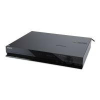
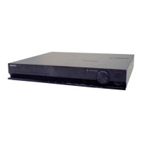
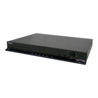
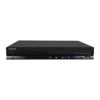
HBD-DZ340M/DZ640M/DZ840K/
DZ840M/DZ940K
(Photo: HBD-DZ940K)