HBD-E370/E470/E570/E870/T57
87
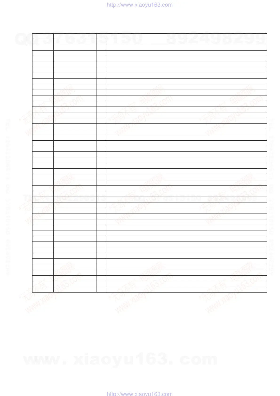
Pin No. Pin Name I/O Description
BA41 DVSS - Ground terminal
BA43 VCC2IO - Power supply terminal (+1.8V)
BB2 SRXN_1 I SATA channel 1 RX differential pair signal (negative) input terminal
BB4 SRXN_2 I SATA channel 2 RX differential pair signal (negative) input terminal Not used
BB6 SVCTST - Not used
BB8 XTAL25MI I System clock signal input terminal (25 MHz)
BB10 TDO - Not used
BB12 TDI - Not used
BB14 VCC2IO - Power supply terminal (+1.8V)
BB16 A_RDQS0B O Data strobe signal (negative) output to the SD-RAM
BB18 VCC2IO - Power supply terminal (+1.8V)
BB20 A_RDQ10 I/O Two-way data bus with the SD-RAM
BB22 VCC2IO - Power supply terminal (+1.8V)
BB24 A_RRASB O Row address strobe signal output to the SD-RAM
BB26 VCC2IO - Power supply terminal (+1.8V)
BB28 A_RBA0 O Bank address signal output to the SD-RAM
BB30 VCC2IO - Power supply terminal (+1.8V)
BB32 A_RDQ17 I/O Two-way data bus with the SD-RAM
BB34 VCC2IO - Power supply terminal (+1.8V)
BB36 A_RDQ31 I/O Two-way data bus with the SD-RAM
BB38 VCC2IO - Power supply terminal (+1.8V)
BB40 A_TP_MEMPLL - Not used
BB42 VCC2IO - Power supply terminal (+1.8V)
BC1 SRXP_1 I SATA channel 1 RX differential pair signal (positive) input terminal
BC3 STXP_1 O SATA channel 1 TX differential pair signal (positive) output terminal
BC5 STXP_2 O SATA channel 2 TX differential pair signal (positive) output terminal Not used
BC7 AVDD33_XTAL25M - Power supply terminal (+3.3V)
BC9 GPIO7 - Not used
BC11 TMS - Not used
BC13 A_RDQ2 I/O Two-way data bus with the SD-RAM
BC15 A_RDQ7 I/O Two-way data bus with the SD-RAM
BC17 A_RDQS1 O Data strobe signal (positive) output to the SD-RAM
BC19 A_RDQ13 I/O Two-way data bus with the SD-RAM
BC21 A_RCLK0 O Clock signal (positive) output to the SD-RAM
BC23 A_RA0 O Address signal output to the SD-RAM
BC25 A_RA6 O Address signal output to the SD-RAM
BC27 A_RA3 O Address signal output to the SD-RAM
BC29 A_RWEB O Write enable signal output to the SD-RAM
BC31 A_RDQ19 I/O Two-way data bus with the SD-RAM
BC33 A_RDQS2B O Data strobe signal (negative) output to the SD-RAM
BC35 A_RDQS3 O Data strobe signal (positive) output to the SD-RAM
BC37 A_RDQ29 I/O Two-way data bus with the SD-RAM
BC39 A_RCLK1B O Clock signal (negative) output to the SD-RAM
BC41 A_TN_MEMPLL - Not used
BC43 A_REXTDN - Not used
w
w
w
.
x
i
a
o
y
u
1
6
3
.
c
o
m
Q
Q
3
7
6
3
1
5
1
5
0
9
9
2
8
9
4
2
9
8
T
E
L
1
3
9
4
2
2
9
6
5
1
3
9
9
2
8
9
4
2
9
8
0
5
1
5
1
3
6
7
3
Q
Q
TEL 13942296513 QQ 376315150 892498299
TEL 13942296513 QQ 376315150 892498299
http://www.xiaoyu163.com
http://www.xiaoyu163.com