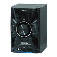
HCD-EC599
32
PANEL BOARD IC100(2/2) LC87F7DJ2CVU-QIP-H (SYSTEM CONTROL)
Pin No. Pin Name I/O Description
1 O-CD-MUTE O CD motor driver ON/OFF mute control signal output for the CD motor/coil driver
2 O-CD-RST O System reset signal output for the CD-MP3 processor
3 I-CD-DO I Serial data input from the CD-MP3 processor
4 O-CD-DI O Serial data output for the CD-MP3 processor
5 O-CD-CLK O Clock signal output for the CD-MP3 processor
6 O-CD-CE O Chip enable signal output for the CD-MP3 processor
7 O-USB-SLEEP O Sleep control signal output for the USB control
8 O-USB-RST O System reset signal output for the USB control
9 I-VBUS-OCP I VBUS overcurrent detection signal input (L:abnormal, H: normal)
10 O-VBUS-ON O VBUS power supply ON/OFF control signal output (L: VBUS off, H: VBUS on)
11 I-RST I Reset signal input
12
SUB-CLK-
IN(32.768KHz)
I Sub system clock signal input (32.768kHz)
13
SUB-CLK-
OUT(32.768KHz)
O Sub system clock signal output (32.768kHz)
14 VSS1 - Ground terminal
15 MAIN-CLK-IN(18MHz) I Main system clock input terminal (18MHz)
16
MAIN-CLK-
OUT(18MHz)
O Main system clock output terminal (18MHz)
17 VDD1 - Power supply pin (+3.3V)
18 I-DEST I Destination setting pin (A/D input)
19 I-CD-AVR I CD protection detection signal input (A/D input)
20 I-KEY-2 I Key signal input (A/D input)
21 I-VBUS-LEVEL-DET I VBUS protection detection signal input (A/D input)
22 I-A+9V-LEVEL-DET I 9V protection detection signal input (A/D input)
23 NC O Not used
24 NC O Not used
25 I-KEY1 I Key signal input (A/D input)
26 I-POWER-KEY I Power key signal input (A/D input)
27 I-AC-MONITOR I AC power monitor input pin (A/D input)
28 I-AC-CUT I AC cut detection signal input (L: AC cut, H: AC In)
29 I-RMC I Remote control signal input from the remove control signal receiver
30 O-STBY-RELAY O Main power on/off control signal output (L: STBY RELAY off, H: STBY RELAY on)
31 O-SPK-RELAY O Relay drive signal output for the speakers (L: SPK RELAY off, H:SPK RELAY on)
32 O-AD-SWITCH O AD Power Control pin (L: Off, H: On)
33 NC O Not used
34 I-PROTECT I Speaker protect detection signal input from speaker protect circuit (L: abnormal, H:normal)
35 I-HP-DET I
Headphone connection detection signal input (L:Headphone disconect, H: Headphone con-
nect)
36 I-VOL-A I Jog dial pulse input A from the MASTER VOLUME encoder
37 I-VOL-B I Jog dial pulse input B from the MASTER VOLUME encoder
38 NC O Not used
39 O-TU-CE O Chip enable signal output for the Tuner
40 NC I Not used
41 I-TU-RDS I RDS Text Detection Signal input
42 NC O Not used
43 NC O Not used
44 NC O Not used
45 to 53 SEG0 to SEG8 O Segment drive signal output for the liquid crystal display panel
54 VDD2 - Power supply pin (+3.3V)
55 VSS2 - Ground terminal
56 to 79 SEG9 to SEG32 O Segment drive signal output for the liquid crystal display panel
80 to 82 LCD V3 to LCD V1 - Bias power supply for the liquid crystal display panel
83 to 86 COM3 to COM0 O Common drive signal output for the liquid crystal display panel
87 O-LCD-LED O LCD back light LED ON/OFF control signal output
88 I-CDM-SW I CD lid open/close detection switch
89 VSS3 - Ground terminal
90 VDD3 - Power supply pin (+3.3V)
91 I2C-TU-DATA I/O Tuner IC data signal for IIC communcation