25
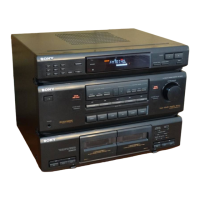
HCD-EP30/EP40
6-11. IC PIN FUNCTION DESCRIPTION
• DISPLAY BOARD IC601 µPD753016AGC-F31-3B9 (SYSTEM CONTROLLER, LIQUID CRYSTAL DISPLAY DRIVER)
Pin No. Pin Name I/O Description
1 to 20 S12 to S31 O Segment drive signal output to the liquid crystal display (D621)
21 to 24 COM0 to COM3 O Common drive signal output to the liquid crystal display (D621)
25 BIAS O Bias output for the liquid crystal display drive
26 to 28 VLC0 to VLC2 I
Input terminal for doubler circuit capacitor connection to develop liquid crystal display drive
voltage
29 TUNER O Power on/off control signal output for the tuner section “L”: power on
30 TAPE O Audio line muting on/off control signal output “L”: muting on
31 CD O Power on/off control signal output for the CD section “L”: power on
32
TIMER STATUS
O LED drive signal output of the TIMER indicator (D619) “L”: LED on
33 VSS — Ground terminal
34 CD-RESET O Reset signal output to the CD section “L”: reset
35 SURROUND O Not used (pull up)
36 PLL CL O PLL serial data transfer clock signal output to the FM/AM PLL (IC102)
37 PLL DI O PLL serial data output to the FM/AM PLL (IC102)
38 TUNER SD I FM and AM signal meter voltage detection input from the LA1823 (IC101)
39 CLOCK O Serial data transfer clock signal output to the LC75392 (IC203)
40 DATA O Serial data output to the LC75392 (IC203)
41 STEREO I FM stereo detection signal input from the LA1823 (IC101) “L”: stereo
42 CD CLOCK I Serial data transfer clock signal input from the CD section
43 RDS CLOCK I
Serial data transfer clock signal input from the RDS decoder (IC604)
(RDS decoder is HCD-EP40 only)
44 REMOTE I Remote control signal input from the remote control receiver (RM601)
45 SYNCRO I Recording on detection signal input
46 MUTE O Audio line muting on/off control signal output “H”: muting on
47 PLLCE O PLL chip enable signal output to the FM/AM PLL (IC102) “H” active
48 CE O Chip enable signal output to the LC75392 (IC203) “H” active
49 SHRST O Not used (open)
50 RDS DATA I Serial data input from the RDS decoder (IC604) (RDS decoder is HCD-EP40 only)
51 PSW O System power on/off control signal out “H”: power on
52 BASS BOOST O Mega bass on/off selection signal output “H”: mega bass on
53 DPSW2/SLEND I
CD lid open/close detection switch (SW600) input terminal “L”: CD lid is closed
54
VDD — Power supply terminal
55 XT1 I Power failure detection input terminal “L”: power failure, “H”: power on
56 XT2 O Not used (open)
57 IC — Internal connection terminal (connected to power supply)
58 X1 I Main system clock input terminal (6 MHz)
59 X2 O Main system clock output terminal (6 MHz)
60 PLLDO SELECT I PLL serial data input from the FM/AM PLL (IC102)
61 CD DATA I/O Two-way data bus with the CD section
62 NC — Not used (open)
63 12/24H SELECT
I
Not used (fixed at “H”)
64 to 67
KEY R0 to
KEY R4
I Key return signal input from the key matrix “L” input when key pressing
68 CPU RESET I
System reset signal input from the reset signal generator (IC603) “L”: reset
For several hundreds msec. after the power supply rises, “L” is input, then it changes to “H”
69 to 80 S0 to S11 O Segment drive signal output to the liquid crystal display (D621)
w
w
w
.
x
i
a
o
y
u
1
6
3
.
c
o
m
Q
Q
3
7
6
3
1
5
1
5
0
9
9
2
8
9
4
2
9
8
T
E
L
1
3
9
4
2
2
9
6
5
1
3
9
9
2
8
9
4
2
9
8
0
5
1
5
1
3
6
7
3
Q
Q
TEL 13942296513 QQ 376315150 892498299
TEL 13942296513 QQ 376315150 892498299
http://www.xiaoyu163.com
http://www.xiaoyu163.com