39
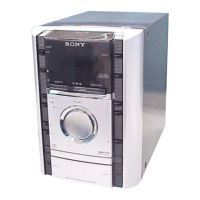
HCD-GS10/GS30DAB
Pin No. Pin Name I/O Description
49 NC — Not used (Open)
50 NC — Not used (Open)
51 MD2 I Input terminal for mode selector (Not used (Fixed to “L”))
52 MD1 I Input terminal for mode selector (Not used (Fixed to “L”))
53 MD0 I Input terminal for mode selector (Not used (Fixed to “L”))
54 RSTX I System reset signal input terminal
55 O-TU-CE O Chip enable signal output to the tuner
56 O-TU-CLK O Clock signal output to the tuner
57 O-TU-DI O Data output to the tuner
58 V3 I Reference power terminal of LCD controller/driver
59 to 62 COM0 to COM3 O Common signal output to the LCD
63, 64 SEG0, SEG1 O Segment signal output to the LCD
65 VCC — Power supply terminal (+3.3V)
66 VSS — Ground terminal
67 to 89 SEG2 to SEG24 O Segment signal output to the LCD
90 VCC — Power supply terminal (+3.3V)
91 VSS — Ground terminal
92 X1 I Resonator input terminal (5.53MHz)
93 X0 O Resonator output terminal (5.53MHz)
94 to 100 SEG25 to SEG31 O Segment signal output to the LCD