HCD-MC1
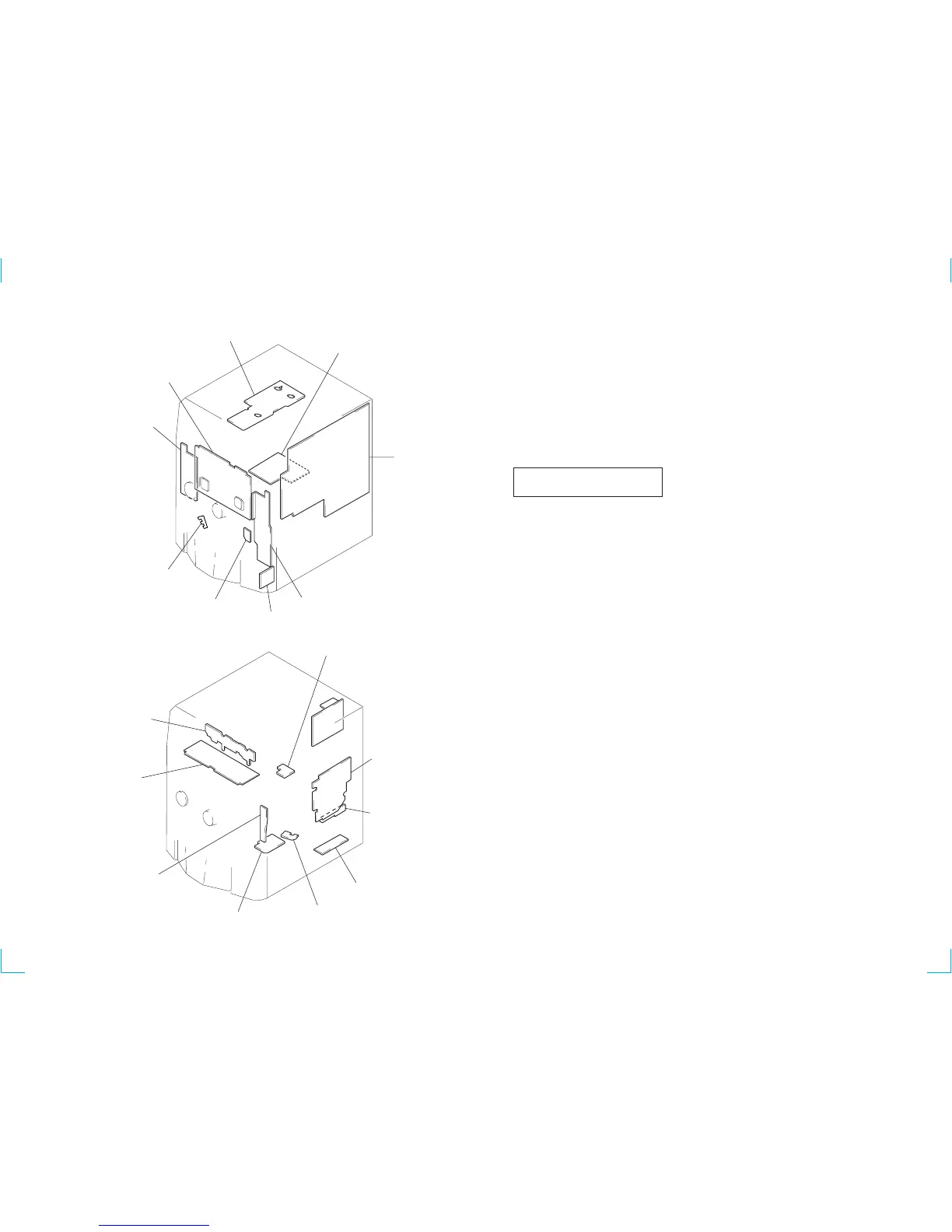
6-2. CIRCUIT BOARD LOCATION
For schematic diagrams.
Note:
• All capacitors are in µF unless otherwise noted. pF: µµF
50 WV or less are not indicated except for electrolytics
and tantalums.
• All resistors are in Ω and
1
/
4
W or less unless otherwise
specified.
• % : indicates tolerance.
•
¢
: internal component.
• 2 : nonflammable resistor.
• 1 : fusible resistor.
• C : panel designation.
• U : B+ Line.
• V : B– Line.
• H : adjustment for repair.
• Voltages and waveforms are dc with respect to ground
under no-signal (detuned) conditions.
• Voltages are taken with a VOM (Input impedance 10 MΩ).
Voltage variations may be noted due to normal produc-
tion tolerances.
• Waveforms are taken with a oscilloscope.
• Circled numbers refer to waveforms.
• Signal path.
F : FM
g : VIDEO/MD
E : PB (DECK A)
d : PB (DECK B)
G : REC (DECK B)
J : CD
c : CD DIGITAL
• Abbreviation
CND : Canadian
THIS NOTE IS COMMON FOR PRINTED WIRING
BOARDS AND SCHEMATIC DIAGRAMS.
(In addition to this necessary note is printed in each
block.)
For printed wiring boards.
Note:
• X : parts extracted from the component side.
•
¢
: internal component.
• b : Pattern from the side which enables seeing.
TABLE SENSOR board
DISC SENSOR (R) board
DOOR SW boar
BD board
CD LED board
AUDIO board
LEAF SW board
CD MOTOR board
DISC SENSOR (S) board
FUNC board
HP/MIC board
POWER AMP board
CD DOOR board
DOOR LED board
SW/POWER board
PANEL board
TRANS board
MAIN board
The components identified by mark ! or dotted
line with mark ! are critical for safety.
Replace only with part number specified.
— 33 — — 34 —