HCD-PZ1D
78
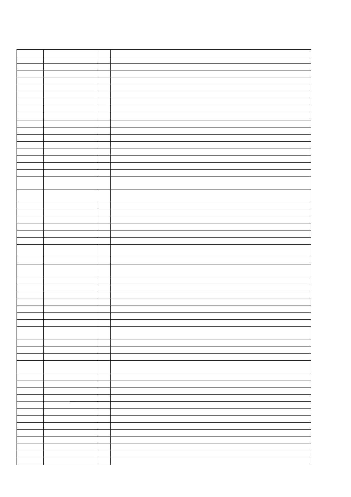
LCD CTRL BOARD IC002 TW8827-TA3-GR (LCD CONTROL)
Pin No. Pin Name I/O Description
1 AVD1 — Power supply pin (+1.8 V)
2 YIN1 I Analog composite signal input 1 (Connect to AVS)
3 YIN0 I Analog composite signal input 0
4 YGND — Ground
5 YOUT O Y signal output (Not used in this set)
6 AVS1 — Ground
7 CIN I Analog component C signal input (Connect to AVS)
8 AVD2 — Power supply pin (+1.8 V)
9 AVS2 — Ground
10 FPBIAS O Flat panel back light bias power on/off control signal output
11 FPPWM1 O Flat panel power monitor signal output (Not used in this set)
12 VDD18_1 — Power supply pin (+1.8 V)
13 VSS18_1 — Ground
14 TCLRL O TCON left/right select signal output (L: right, H: left)
15 FPPWC O Flat panel power on/off control signal output
16 TRCLK O TCON row driver shift clock signal output
17 TRUDL/GPO1 O TCON up/down select signal output (L: down, H: up)/general purpose signal output
18 TCINV/GPO2 O
TCON column driver inversion signal output/general purpose signal output (Not used in this
set)
19 POL_A/GPO3 O
TCON column driver polarity A signal output/general purpose signal output (Not used in this
set)
20 POL_B/GPO4 O TCON column driver polarity B signal output/general purpose signal output
21 TCLP O TCON column driver load pulse signal output
22 FPCLK O Flat panel clock signal output
23 VDD33_1 — Power supply pin (+3.3 V)
24 VSS33_1 — Ground
25 TRSPT/FPVS O TCON row driver starting pulse (top start) signal output/fl at panel vertical sync signal output
26 TCSPL/FPHS O
TCON column driver starting pulse (left to right scan) signal output/fl at panel horizontal sync
signal output
27 TROE/FPDE O TCON row driver output enable signal output/fl at panel data valid signal output
28 TCSPR/GPO5 O
TCON column driver starting pulse (right to left scan) signal output/general purpose signal
output
29 TRSPB/GPO6 O TCON row driver starting pulse (bottom start) signal output/general purpose signal output
30 to 33 DTV0 to DTV3 I DTV signal input 0 to 3 (Not used in this set)
34 VDD18_2 — Power supply pin (+1.8 V)
35 VSS18_2 — Ground
36 to 39 DTV4 to DTV7 I/O DTV signal input 4 to 7 (Not used in this set)
40 VDD33_2 — Power supply pin (+3.3 V)
41 VSS33_2 — Ground
42 to 49
DTV8/P2.0 to DTV15/
P2.7
I/O DTV signal input 8 to 15/MCU port signal input 2.0 to 2.7 (Not used in this set)
50 DTVCLK I/O DTV interface clock signal input (Not used in this set)
51 DTVVS I/O DTV interface vertical sync signal input (Not used in this set)
52 DTVHS I/O DTV interface horizontal sync signal input (Not used in this set)
53 DTVDE/P3.2/INT I/O
DTV interface data valid signal input/MCU port signal input 3.2 (MCU int0) (Not used in this
set)
54 XOUT O System clock signal output (27 MHz)
55 XIN I System clock signal input (27 MHz)
56 RESET I Reset signal input
57 TEST1 I Production test pin (Connect to VSS33)
58 VDD33_3 — Power supply pin (+3.3 V)
59 VSS33_3 — Ground
60 PWR_DN I Power down signal input (Connect to VSS33)
61 MCU_EN I MCU enable signal input (Fixed at L in this set)
62 SDAT/P1.1 I/O 2-wire IIC interface data input/output//MCU port signal input/output 1.1
63 SCLK/P1.0 I/O 2-wire IIC interface clock signal input/output//MCU port signal input/output 1.1
64 RXD/P3.0 I/O MCU RXD signal input/MCU port signal input 3.0 (Not used in this set)
65 TXD/P3.1 I/O MCU TXD signal output/MCU port signal output 3.1 (Not used in this set)
66 VDD18_3 — Power supply pin (+1.8 V)


 To Next Page