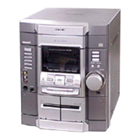
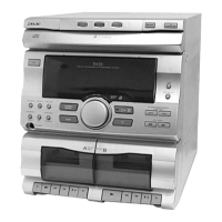
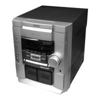
HCD-RB5
1111
SECTION 5
DIAGRAMS
NOTE FOR PRINTED WIRING BOARDS AND SCHEMATIC DIAGRAMS
Note on Printed Wiring Board:
• X : parts extracted from the component side.
•
f
: internal component.
• b : Pattern from the side which enables seeing.
Caution:
Pattern face side: Parts on the pattern face side seen from
(Side B) the pattern face are indicated.
Parts face side: Parts on the parts face side seen from
(Side A) the parts face are indicated.
Note on Schematic Diagram:
• All capacitors are in µF unless otherwise noted. pF: µµF
50 WV or less are not indicated except for electrolytics
and tantalums.
• All resistors are in Ω and
1
/
4
W or less unless otherwise
specified.
•
f
: internal component.
• 2 : nonflammable resistor.
• 5 : fusible resistor.
• C : panel designation.
• U : B+ Line.
• V : B– Line.
• H : adjustment for repair.
• Voltages are taken with a VOM (Input impedance 10 MΩ).
Voltage variations may be noted due to normal produc-
tion tolerances.
• Waveforms are taken with a oscilloscope.
Voltage variations may be noted due to normal produc-
tion tolerances.
• Circled numbers refer to waveforms.
• Signal path.
F : TUNER (FM/AM)
J : CD PLAY (ANALOG OUT)
c : CD PLAY (DIGITAL OUT)
• Abbreviation
CND : Canadian model.
AUS : Australian model.
SP : Singapore model.
MY : Malaysia model.
AR : Argentine model.
AED : North European model.
MX : Mexican model.
KR : Korean model.
EE : East European model.
HK : Hong Kong model.
TW : Taiwan model.
CH : Chinese model.
• Indication of transisitor.
C
B
These are omitted.
E
Q
B
These are omitted.
CE
Q
B
These are omitted.
CE
Q
The components identified by
mark 0 or dotted line with mark
0 are critical for safety.
Replace only with part number
specified.
Les composants identifiés par
une marque 0 sont critiques
pour la sécurité.
Ne les remplacer que par une
pièce portant le numéro spécifié.
5-2. CIRCUIT BOARDS LOCATION
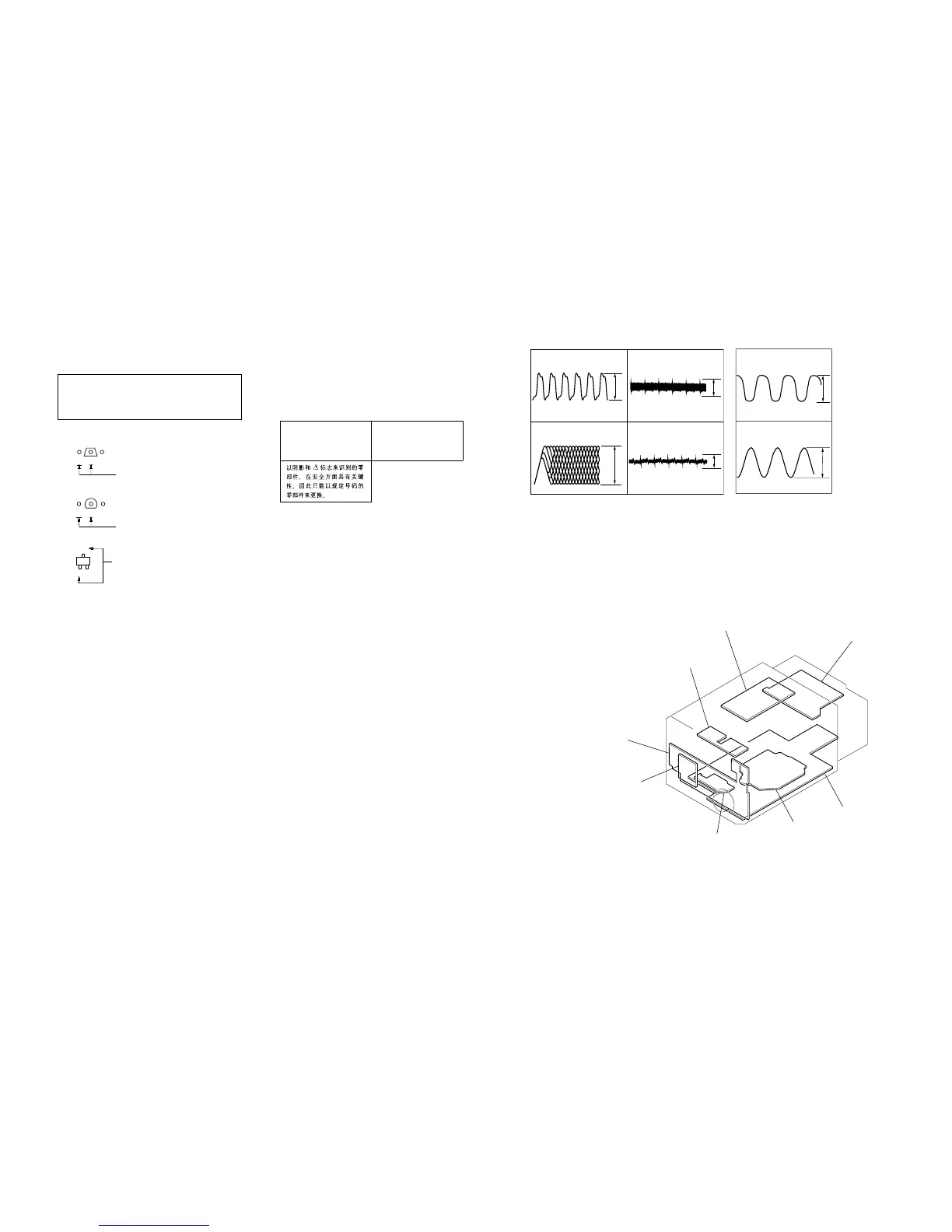
5-1. Wavefoarms
1 IC101 yj
CD PLAY MODE
6.4Vp-p
16.9344MHz
1.2Vp-p
2 IC101 ta
CD PLAY MODE
3 IC101 ra
CD PLAY MODE
4 IC101 el
CD PLAY MODE
400nsec/div
approx 200mVp-p
approx 170mVp-p
1 IC601 qa
STOP MODE
3.0Vp-p
32.768kHz
3.4Vp-p
2 IC601 qd
STOP MODE
16MHz
– BD BOARD – – MAIN BOARD –
BACK PANEL board
LED board
PANEL board
H.P. board
LOADING board
BD board
MAIN board
TUNER (FM/AM) UNIT