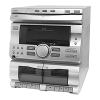
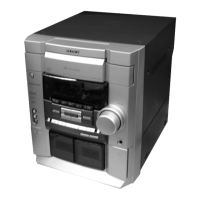
2
TABLE OF CONTENTS
The laser diode in the optical pick-up block may suffer electrostatic
break-down because of the potential difference generated by the
charged electrostatic load, etc. on clothing and the human body.
During repair, pay attention to electrostatic break-down and also
use the procedure in the printed matter which is included in the
repair parts.
The flexible board is easily damaged and should be handled with
care.
NOTES ON LASER DIODE EMISSION CHECK
The laser beam on this model is concentrated so as to be focused on
the disc reflective surface by the objective lens in the optical pick-
up block. Therefore, when checking the laser diode emission,
observe from more than 30 cm away from the objective lens.
Notes on chip component replacement
• Never reuse a disconnected chip component.
• Notice that the minus side of a tantalum capacitor may be dam-
aged by heat.
Flexible Circuit Board Repairing
• Keep the temperature of the soldering iron around 270 ˚C dur-
ing repairing.
• Do not touch the soldering iron on the same conductor of the
circuit board (within 3 times).
• Be careful not to apply force on the conductor when soldering
or unsoldering.
NOTES ON HANDLING THE OPTICAL PICK-UP
BLOCK OR BASE UNIT
CAUTION
Use of controls or adjustments or performance of procedures
other than those specified herein may result in hazardous
radiation exposure.
This appliance is classified as a CLASS 1 LASER product.
The CLASS 1 LASER PRODUCT MARKING is located on
the rear exterior.
Laser component in this product is capable of emitting radiation
exceeding the limit for Class 1.
1. GENERAL ·········································································· 4
2. DISASSEMBLY ································································ 6
3. SERVICE MODE ······························································ 9
4. ELECTRICAL ADJUSTMENTS ······························· 10
5. DIAGRAMS
5-1. Wavefoams ·································································· 11
5-2. Circuit Boards Location ·············································· 11
5-3. PRINTED WIRING BOARD –BD SECTION– ······· 12
5-4. SCHEMATIC DIAGRAM –BD SECTION–············ 13
5-5. PRINTED WIRING BOARDS
–MAIN SECTION– ··················································· 14
5-6. SCHEMATIC DIAGRAM
–MAIN SECTION(1/2)– ··········································· 15
5-7. SCHEMATIC DIAGRAM
–MAIN SECTION(2/2)– ··········································· 16
5-8. PRINTED WIRING BOARDS
–POWER SECTION– ················································ 17
5-9. PRINTED WIRING BOARD
–PANEL SECTION– ················································· 18
5-10. SCHEMATIC DIAGRAM
–PANEL SECTION– ················································· 19
5-11. SCHEMATIC DIAGRAM
–LOADING SECTION– ············································ 20
5-12. PRINTED WIRING BOARDS
–LOADING SECTION– ············································ 20
5-13. IC Pin Function ·························································· 20
5-14. IC Block Diagrams····················································· 22
6. EXPLODED VIEWS ................................................... 23
7. ELECTRICAL PARTS LIST ................................... 28