55
HCD-RV22/RV55
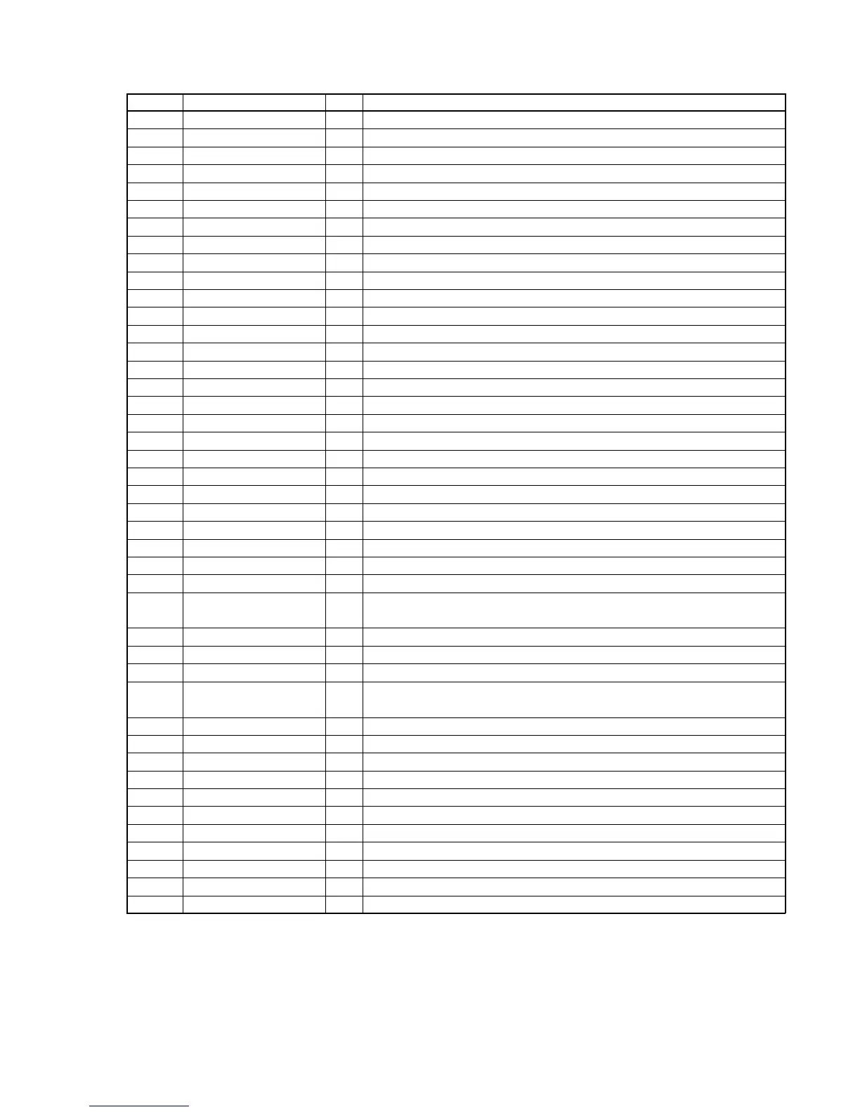
Pin No. Pin Name I/O Pin Description
158 AVS0 — Analog ground pin
159 ADIO O Output for the test Not used.
160 RFDC I RF signal input from the RF amplifier
161 CE I Center servo analog signal input
162 TE I Tracking error signal input from the RF amplifier
163 SE I Sled error signal input from the RF amplifier
164 FE I Focus error signal input from the RF amplifier
165 VC I Center voltage (+1.65 V) input
166 VPCO O Wide-band EFM PLL charge pump output
167 VCTL I Wide-band EFM PLL VCO2 control voltage input
168 FILO O Master PLL filter output
169 FILI I Master PLL filter input
170 PCO O Master PLL charge pump output
171 CLTV I Multiplier VCO1 control voltage input
172 AVS1 — Analog ground pin
173 RFAC I EFM signal input from the RF amplifier
174 BIAS I Asymmetry circuit constant current input
175 ASYI I Asymmetry comparator voltage input
176 ASYO O EFM full-swing output
177 AVD1 — Analog power supply pin (2.5 V)
178 VDD7 — Digital power supply pin (+2.5 V) (for CD-DSP block)
179 SOUT O Serial data output Not used. (Open)
180 SOCK O Serial data readout clock signal output Not used. (Open)
181 XOLT O Serial data latch pulse signal output Not used. (Open)
182 C4M O 4.2336 MHz clock signal output Not used. (Open)
183 LOCK O GFS is sampled by 460 Hz “H” output when GFS is “H”
184 VSS7 — Digital ground pin
185 MD2 I
Digital out on/off control signal input “L”: digital out off, “H”: digital out on
Not used. (Fixed at “L”.)
186 SCSY I Guard subcode sync (S0+S1) resynchronization input Not used. (Fixed at “L”.)
187 PWMI I Spindle motor external control signal input Not used. (Fixed at “L”.)
188 VDD8 — Digital power supply pin (+2.5 V) (for CD-DSP block )
189 XTSL I
Input for the system clock frequency setting
“L”: 16.9344 MHz, “H”: 33.8688 MHz Fixed at “H” in this set
190 VSS8 — Digital ground pin
191 PVS2 — Analog ground pin (for PLL2)
192 LPFI I Connected of PLL2 filter
193 LPFO O Connected of PLL2 filter
194 PVD2 — Analog power supply pin (+2.5 V) (for PLL2)
195, 196 NC — Not used. (Open)
197 PVD1 — Analog power supply pin (+2.5 V) (for PLL1)
198 PVS1 — Analog ground pin (for PLL1)
199 TMODE0 I Selection signal input for the test Not used. (Fixed at “L”.)
200 AUDDTI I Serial audio data input Not used. (Fixd at “L”.)
201 AUDDTO0 O Serial audio data output to the digital filter


 To Next Page