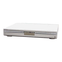
HCD-S550/S880
4
TABLE OF CONTENTS
SELF DIAGNOSIS FUNCTION .................................... 2
1. SERVICING NOTES ............................................... 5
2. GENERAL
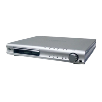
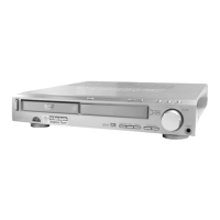
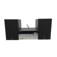
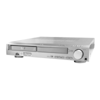
Location of Controls ...................................................... 6
3. DISASSEMBLY
3-1. Disassembly Flow .......................................................... 9
3-2. Front Panel Section, Side Panel (L)/(R) ........................ 10
3-3. I/O Board......................................................................... 10
3-4. SEL Board ....................................................................... 11
3-5. DVD Board...................................................................... 11
3-6. Mechanism Deck Section (CDM72B-DVBU12) .......... 12
3-7. POWER SW Board, DDCON Board............................. 12
3-8. Power Board ................................................................... 13
3-9. AMP Board .................................................................... 13
3-10. Optical Pick-up (DVBU12) ........................................... 14
3-11. RELAY Board ................................................................ 14
3-12. Holder (AT) Assy, Retainer (Chassis) Block................. 15
3-13. Belt (L2) ......................................................................... 15
3-14. Pulley (RTR) Assy ......................................................... 16
3-15. Belt (CK) ........................................................................ 16
3-16. Pulley (SPT) Assy .......................................................... 17
3-17. Belt (CK), Motor (CK) Assy (M751) ............................ 17
4. ASSEMBLY
4-1. How to Install Pulley (SPT) Assy .................................. 18
4-2. How to Install Pulley (RTR) Assy ................................. 18
4-3. How to Install Rotary Encoder (Mode) (S741) ............. 19
5. TEST MODE............................................................. 20
6. ELECTRICAL ADJUSTMENT........................... 27
7. DIAGRAMS
7-1. Block Diagram – RF SERVO Section – ....................... 28
7-2. Block Diagram – AUDIO (DSP) Section – .................. 29
7-3. Block Diagram – AUDIO OUT, PANEL Section – ..... 30
7-4. Block Diagram – VIDEO Section – ............................. 31
7-5. Block Diagram – MECHANISM DECK,
POWER SUPPLY Section – .......................................... 32
7-6. Note for Printed Wiring Boards and
Schematic Diagrams ...................................................... 33
7-7. Printed Wiring Boards – RF Section – ......................... 34
7-8. Schematic Diagram – RF Section –.............................. 35
7-9. Printed Wiring Boards
– MECHANISM DECK Section – ................................ 36
7-10. Schematic Diagram
– MECHANISM DECK Section – ................................ 37
7-11. Printed Wiring Board
– DVD Board (Component Side) – ............................... 38
7-12. Printed Wiring Board
– DVD Board (Conductor Side) – ................................. 39
7-13. Schematic Diagram – DVD Board (1/10) – ................. 40
7-14. Schematic Diagram – DVD Board (2/10) – ................. 41
7-15. Schematic Diagram – DVD Board (3/10) – ................. 42
7-16. Schematic Diagram – DVD Board (4/10) – ................. 43
7-17. Schematic Diagram – DVD Board (5/10) – ................. 44
7-18. Schematic Diagram – DVD Board (6/10) – ................. 45
7-19. Schematic Diagram – DVD Board (7/10) – ................. 46
7-20. Schematic Diagram – DVD Board (8/10) – ................. 47
7-21. Schematic Diagram – DVD Board (9/10) – ................. 48
7-22. Schematic Diagram – DVD Board (10/10) – ............... 49
7-23. Printed Wiring Board – AMP Section (1/2) – .............. 50
7-24. Printed Wiring Boards – AMP Section (2/2) –............. 51
7-25. Schematic Diagram – AMP Section (1/2) – ................. 52
7-26. Schematic Diagram – AMP Section (2/2) – ................. 53
7-27. Printed Wiring Board – I/O Section (1/2) – .................. 54
7-28. Printed Wiring Boards – I/O Section (2/2) –................ 55
7-29. Schematic Diagram – I/O Section (1/2) – .................... 56
7-30. Schematic Diagram – I/O Section (2/2) – .................... 57
7-31. Printed Wiring Boards
– DC-DC CONVERTER Section – ............................... 58
7-32. Schematic Diagram
– DC-DC CONVERTER Section – ............................... 59
7-33. Printed Wiring Boards – CONTROL Section – ........... 60
7-34. Schematic Diagram – CONTROL Section –................ 61
7-35. Printed Wiring Board – FL Board – ............................. 62
7-36. Schematic Diagram – FL Board – ................................ 63
7-37. Printed Wiring Board – POWER Section (1/2) –......... 64
7-38. Printed Wiring Boards – POWER Section (2/2) – ....... 65
7-39. Schematic Diagram – POWER Section – .................... 66
7-40. IC Pin Function Description .......................................... 84
8. EXPLODED VIEWS
8-1. General Section ............................................................. 102
8-2. Front Panel Section-1.................................................... 103
8-3. Front Panel Section-2.................................................... 104
8-4. Chassis Section-1 .......................................................... 105
8-5. Chassis Section-2 .......................................................... 106
8-6. Chassis Section-3 .......................................................... 107
8-7. Chassis Section-4 .......................................................... 108
8-8. Mechanism Deck Section-1 (CDM72B-DVBU12)...... 109
8-9. Mechanism Deck Section-2 (CDM72A-DVBU12) ..... 110
8-10. Mechanism Deck Section-3 (CDM72A-DVBU12) ..... 111
8-11. Mechanism Deck Section-4 (CDM72A-DVBU12) ..... 112
8-12. Mechanism Deck Section-5 (CDM72A-DVBU12) ..... 113
8-13. Mechanism Deck Section-6 (CDM72A-DVBU12) ..... 114
8-14. Mechanism Deck Section-7 (CDM72A-DVBU12) ..... 115
8-15. Optical Pick-up Section (DVBU12) ............................. 116
9. ELECTRICAL PARTS LIST ............................. 117
Ver 1.4