EasyManua.ls Logo

Sony HCD-XGV10AV User Manual

Sony HCD-XGV10AV
94 pages
To Next Page IconTo Next Page
Page #1 background imageLoading...
Page #1 background image
HCD-XGV6/XGV8/XGV10AV
E Model
COMPACT Hi-Fi STEREO SYSTEM
— Continued on next page —
SPECIFICATIONS
HCD-XGV6/XGV8/XGV10AV are the
Amplifier, CD player, tape deck and
tuner section in LBT-XGV6/XGV8/
XGV10AV.
Ver 1.2 2004.09
9-873-959-03
2004I02-1
© 2004.09
Model Name Using Similar Mechanism NEW
CD CD Mechanism Type CDM37B-30BD62
Section Base Unit Name BU-30BD62
Optical Pick-up Name A-MAX.3
TAPE
Model Name Using Similar Mechanism HCD-XGR90AV
Section
SERVICE MANUAL
Sony Corporation
Audio Group
Published by Sony Engineering Corporation
Photo : HCD-XGV10AV
Amplifier section
LBT-XGV10AV
Front Speaker:
The following measured at AC 120/220/240 V, 50 Hz
DIN power output (Rated) 150 + 150 watts
(6 ohms at 1 kHz, DIN)
Continuous RMS power output (Reference)
200 + 200 watts
(6 ohms at 1 kHz, 10% THD)
Center Speaker:
DIN power output (Rated) 35 watts
(8 ohms at 1 kHz, DIN)
Continuous RMS power output (Reference)
50 watts
(8 ohms at 1 kHz, 10% THD)
Rear Speaker:
DIN power output (Rated) 35 + 35 watts
(8 ohms at 1 kHz, DIN)
Continuous RMS power output (Reference)
50 + 50 watts
(8 ohms at 1 kHz, 10% THD)
LBT-XGV8
The following measured at AC 120/220/240V, 50 Hz
DIN power output (rated) 125W x 2 + 125W x 2
(6 ohms at 1 kHz, DIN)
Continuous RMS power output (reference)
170 W x 2 + 170 W x 2
(6 ohms at 1 kHz, 10% THD)
LBT-XGV6
The following measured at AC 120/220/240V, 50 Hz
DIN power output (rated) 150 + 150 watts (6 ohms at 1 kHz, DIN)
Continuous RMS power output (reference)
200 + 200 watts (6 ohms at 1 kHz,
10% THD)
Inputs
PHONO IN:
(phono jacks) sensitivity 3 mV,
impedance 47 kilohms
MIC1/2:
(phone jacks) sensitivity 1 mV,
impedance 10 kilohms
GAME INPUT:
(phono jacks) sensitivity 250 mV,
impedance 47 kilohms
MD (VIDEO) IN:
(phono jack) sensitivity 450 mV
(250 mV),
impedance 47 kilohms
DVD INPUT (XGV10AV)
FRONT, REAR, CENTER, WOOFER (phono jacks):
sensitivity 450 mV,
impedance 47 kilohms

Table of Contents

Question and Answer IconNeed help?

Do you have a question about the Sony HCD-XGV10AV and is the answer not in the manual?

Sony HCD-XGV10AV Specifications

General IconGeneral
BrandSony
ModelHCD-XGV10AV
CategoryStereo System
LanguageEnglish

Summary

SPECIFICATIONS

Model and Specification Details

Technical specifications for different models and system inputs.

SECTION 1 SERVICING NOTE

Jig for Prologic Board Checking

Details on the special jig for checking the PROLOGIC board.

SECTION 2 GENERAL

Main Unit Overview Diagram

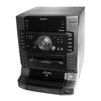
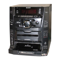
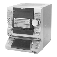
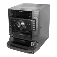
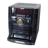
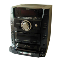
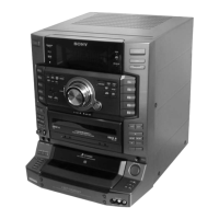
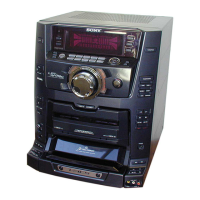
Diagram identifying controls and components of the main unit.

Remote Control Operation (For XGV10AV)

Button Functions and Operation

Description of remote control buttons and their operations.

Remote Control Operation (For XGV6, XGV8)

Button Functions and Operation

Description of remote control buttons and their operations.

SECTION 3 DISASSEMBLY

Case Removal Procedure

Step-by-step guide for removing the outer case.

DISASSEMBLY

Front Panel and Tape Mechanism Removal

Procedures for disassembling the front panel and tape deck.

DISASSEMBLY

Panel Boards Disassembly

Disassembly steps for Panel FL, TC-A, TC-B, and Panel VR boards.

DISASSEMBLY

Input Boards Disassembly

Disassembly steps for MIC/Guitar, Headphone, and Front Input boards.

DISASSEMBLY

Disc-Related and Rear Boards Disassembly

Disassembly of D-SW, CD-L, CD-R boards, and back panel assemblies.

DISASSEMBLY

CD Mechanism Deck Disassembly

Procedure for removing the CD mechanism deck assembly.

DISASSEMBLY

Base Unit Disassembly

Disassembly steps for Base Unit-1 and Base Unit-2.

DISASSEMBLY

BD Board and Disc Table Procedures

Disassembly of BD board and disc table adjustment.

SECTION 4 TEST MODE

System Reset and Configuration Modes

Procedures for system resets, tuning intervals, and function name changes.

CD Pickup and System Operation Tests

Tests for CD pickup, LEDs, and aging operations.

SECTION 5 MECHANICAL ADJUSTMENTS

Torque Measurement Details

Specifies torque values for various mechanical adjustments.

SECTION 6 ELECTRICAL ADJUSTMENTS

Test Tape Specifications

Lists test tapes and signals for electrical adjustments.

CD SECTION

CD Performance Checks

Procedures for S-Curve, RF Level, and E-F Balance checks.

VIDEO SECTION

Video Level Adjustment

Procedure for adjusting video output level.

SECTION 7 DIAGRAMS

Circuit Board Location Overview

Diagram showing physical placement of all circuit boards.

BLOCK DIAGRAMS

CD Servo Section Block Diagram

Block diagram illustrating the CD servo control system.

BLOCK DIAGRAMS

Tuner/Tape Deck and Main Section Block Diagrams

Block diagrams for tuner, tape deck, and main processing sections.

BLOCK DIAGRAMS

Display, Power Supply Block Diagram

Block diagram of display, key control, and power supply systems.

PRINTED WIRING BOARD - BD SECTION

BD Board Component Layout

Component placement diagram for the BD board (Sides A & B).

SCHEMATIC DIAGRAM - BD SECTION

BD Board Electrical Schematic

Electrical schematic diagram for the BD board.

SCHEMATIC DIAGRAM - VIDEO SECTION

Video Section Schematic (Part 1)

Electrical schematic for the video section, first part.

SCHEMATIC DIAGRAM - VIDEO SECTION

Video Section Schematic (Part 2)

Electrical schematic for the video section, second part.

PRINTED WIRING BOARD - VIDEO SECTION

Video Board Component Layout

Component placement diagram for the video board (Sides A & B).

MOTOR, LED SECTION

Motor, LED Boards Schematics and Layout

Component layout and schematics for motor and LED sections.

SCHEMATIC DIAGRAM - MAIN SECTION

Main Board Schematic (Part 1)

Electrical schematic for the main board, first part.

SCHEMATIC DIAGRAM - MAIN SECTION

Main Board Schematic (Part 2)

Electrical schematic for the main board, second part.

SCHEMATIC DIAGRAM - MAIN SECTION

Main Board Schematic (Part 3)

Electrical schematic for the main board, third part.

PRINTED WIRING BOARD - MAIN SECTION

Main Board Component Layout

Component placement diagram for the main board.

PRINTED WIRING BOARD - CD-L, CD-R, HEADPHONE, FRONT INPUT, D-SW SECTION

CD-L, CD-R, Headphone, Front Input, D-SW Boards Layout

Component layout for multiple small boards related to disc and input.

SCHEMATIC DIAGRAM - CD-L, CD-R, HEADPHONE, FRONT INPUT, D-SW SECTION

CD-L, CD-R, Headphone, Front Input, D-SW Schematics

Electrical schematics for multiple small boards related to disc and input.

PRINTED WIRING BOARD - PANEL VR SECTION

Panel VR Board Component Layout

Component placement diagram for the Panel VR board.

SCHEMATIC DIAGRAM - PANEL VR SECTION

Panel VR Board Electrical Schematic

Electrical schematic for the Panel VR board.

PRINTED WIRING BOARD - PANEL FL, TC-A, TC-B SECTION

Panel FL, TC-A, TC-B Boards Layout

Component layout for display and audio control boards.

SCHEMATIC DIAGRAM - PANEL FL, TC-A, TC-B SECTION

Panel FL, TC-A, TC-B Boards Schematics

Electrical schematics for display and audio control boards.

PRINTED WIRING BOARD - PA SECTION (XGV10AV)

PA Board Component Layout (XGV10AV)

Component layout for the PA board used in XGV10AV model.

SCHEMATIC DIAGRAM - PA SECTION (XGV10AV)

PA Board Electrical Schematic (XGV10AV)

Electrical schematic for the PA board used in XGV10AV model.

PRINTED WIRING BOARD - PA SECTION (XGV6/XGV8)

PA Board Component Layout (XGV6/XGV8)

Component layout for the PA board used in XGV6/XGV8 models.

SCHEMATIC DIAGRAM - PA SECTION (XGV6/XGV8)

PA Board Electrical Schematic (XGV6/XGV8)

Electrical schematic for the PA board used in XGV6/XGV8 models.

SCHEMATIC DIAGRAM - SUB AMP SECTION (XGV10AV)

Sub Amp Board Schematic (XGV10AV)

Electrical schematic for the Sub Amp board in XGV10AV.

SCHEMATIC DIAGRAM - SUB AMP SECTION (XGV8)

Sub Amp Board Schematic (XGV8)

Electrical schematic for the Sub Amp board in XGV8.

PRINTED WIRING BOARD - SUB AMP SECTION (XGV10AV/XGV8)

Sub Amp Board Component Layout (XGV10AV/XGV8)

Component layout for the Sub Amp board in XGV10AV/XGV8.

MIC/GUITAR SECTION

Schematics and Printed Wiring Board Layout

Electrical schematics and component layout for the MIC/Guitar section.

PRINTED WIRING BOARD - PROLOGIC SECTION (XGV10AV)

Prologic Board Component Layout (XGV10AV)

Component layout for the Prologic board in XGV10AV.

SCHEMATIC DIAGRAM - PROLOGIC SECTION (XGV10AV)

Prologic Board Electrical Schematic (XGV10AV)

Electrical schematic for the Prologic board in XGV10AV.

TRANS, SUB TRANS SECTION

Schematics and Printed Wiring Board Layout

Component layout and schematics for TRANS and SUB TRANS boards.

WAVEFORMS

Waveform Diagrams

Visual representations of key signal waveforms from various ICs.

IC PIN FUNCTIONS

IC505 CXD1887R Pinout Details

Detailed pin description for IC505 on the VIDEO board.

IC PIN FUNCTIONS

IC505 CXD1887R Pinout Details Continued

Continued pin description for IC505 on the VIDEO board.

IC PIN FUNCTIONS

IC505 CXD1887R Pinout Details Continued

Continued pin description for IC505 on the VIDEO board.

IC PIN FUNCTIONS

IC505 CXD1887R Pinout Details Continued

Continued pin description for IC505 on the VIDEO board.

IC PIN FUNCTIONS

IC501 M30620MCN Pinout Details

Detailed pin description for IC501 on the MAIN board.

IC PIN FUNCTIONS

IC501 M30620MCN Pinout Details Continued

Continued pin description for IC501 on the MAIN board.

IC PIN FUNCTIONS

IC601 MB90M407APF Pinout Details

Detailed pin description for IC601 on the PANEL FL board.

IC BLOCK DIAGRAMS

IC103 CXA2581N Block Diagram

Block diagram illustrating the function of IC103 on the BD board.

IC BLOCK DIAGRAMS

IC102 AN41020A Block Diagram

Block diagram illustrating the function of IC102 on the BD board.

IC BLOCK DIAGRAMS

Multiple IC Block Diagrams

Block diagrams for various ICs across different boards.

IC BLOCK DIAGRAMS

Multiple IC Block Diagrams

Block diagrams for various ICs across different boards.

EXPLODED VIEWS

Case and Back Panel Exploded View

Exploded diagram of the unit's case and back panel assembly.

FRONT PANEL SECTION-1

Front Panel Section-1 Exploded View

Exploded diagram of the front panel components, part 1.

FRONT PANEL SECTION-2

Front Panel Section-2 Exploded View

Exploded diagram of the front panel components, part 2.

CHASSIS SECTION

Chassis Section Exploded View

Exploded diagram of the main chassis assembly and related parts.

CD MECHANISM DECK SECTION

CD Mechanism Deck Exploded View

Exploded diagram of the CD mechanism deck assembly.

BASE UNIT SECTION

Base Unit Section Exploded View

Exploded diagram of the Base Unit assembly.

ELECTRICAL PARTS LIST

BD and CD-L Board Parts List

List of electrical components for the BD and CD-L boards.

ELECTRICAL PARTS LIST

Main and Other Boards Parts List

List of electrical components for multiple boards including Main, Headphone, etc.

ELECTRICAL PARTS LIST

Main Board Capacitors List

Detailed list of capacitors used on the Main board.

ELECTRICAL PARTS LIST

Main Board Capacitors List

Detailed list of capacitors used on the Main board.

ELECTRICAL PARTS LIST

Main Board Transistors and Resistors List

List of transistors and resistors for the Main board.

ELECTRICAL PARTS LIST

Main Board Resistors List

Detailed list of resistors used on the Main board.

ELECTRICAL PARTS LIST

Main Board Resistors List

Detailed list of resistors used on the Main board.

ELECTRICAL PARTS LIST

Main, Mic/Guitar, and Motor Boards Parts List

List of components for Main, Mic/Guitar, and Motor boards.

ELECTRICAL PARTS LIST

Mic/Guitar, Motor, PA Boards Parts List

List of components for Mic/Guitar, Motor, and PA boards.

ELECTRICAL PARTS LIST

PA Board Diodes and Transistors List

List of diodes and transistors for the PA board.

ELECTRICAL PARTS LIST

PA Board Resistors List

Detailed list of resistors used on the PA board.

ELECTRICAL PARTS LIST

PA and Panel FL Boards Parts List

List of components for the PA and Panel FL boards.

ELECTRICAL PARTS LIST

Panel FL and Panel VR Boards Parts List

List of components for the Panel FL and Panel VR boards.

ELECTRICAL PARTS LIST

Panel VR Board Components List

List of components for the Panel VR board.

ELECTRICAL PARTS LIST

Panel VR and Prologic Boards Parts List

List of components for the Panel VR and Prologic boards.

ELECTRICAL PARTS LIST

TC-B, Trans, and Video Boards Parts List

List of components for TC-B, Trans, and Video boards.

ELECTRICAL PARTS LIST

Sub Amp, Sub Trans, TC-A, TC-B Boards Parts List

List of components for Sub Amp, Sub Trans, TC-A, and TC-B boards.

ELECTRICAL PARTS LIST

TC-B, Trans, and Video Boards Parts List

List of components for TC-B, Trans, and Video boards.

ELECTRICAL PARTS LIST

Video Board Components List

Detailed list of components for the Video board.

ELECTRICAL PARTS LIST

Video Board Components List

Detailed list of components for the Video board.

REVISION HISTORY

Revision Details

Summary of changes made across manual revisions.

Related product manuals