EasyManua.ls Logo

Sony HCD-XG900AV User Manual

Sony HCD-XG900AV
86 pages
To Next Page IconTo Next Page
Page #1 background imageLoading...
Page #1 background image
SERVICE MANUAL
COMPACT DISC DECK RECEIVER
AEP Model
UK Model
HCD-XG900AV
E Model
Australian Model
HCD-XG100AV
SPECIFICATIONS
HCD-XG100AV/XG900AV
Photo: HCD-XG900AV
Ver 1.1 2002.10
9-873-815-12 Sony Corporation
2002J0500-1 Home Audio Company
C 2002.10 Published by Sony Engineering Corporation
HCD-XG100AV/XG900AV are the amplifier,
CD player, tape deck and tuner section in
LBT-XG100AV/XG900AV.
Model Name Using Similar Mechanism HCD-XG80
CD
CD Mechanism Type CDM37M-5BD32L
Section
Base Unit Name BU-5BD32L
Optical Pick-up Name KSS-213DH
TAPE
Model Name Using Similar Mechanism HCD-XG80
Section
Tape Transport Mechanism Type TCM-230PWR42
– Continued on next page –
Amplifier section
HCD-XG900AV
Front Speaker:
DIN power output (Rated)
90 + 90 watts
(6 ohms at 1 kHz, DIN)
Continuous RMS power output (Reference)
120 + 120 watts
(6 ohms at 1 kHz, 10%
THD)
Music power output (Reference)
200 + 200 watts
(6 ohms at 1 kHz, 10%
THD)
Center Speaker:
DIN power output (Rated)
30 watts
(8 ohms at 1 kHz, DIN)
Continuous RMS power output (Reference)
40 watts
(8 ohms at 1 kHz, 10%
THD)
Music power output (Reference)
60 watts
(8 ohms at 1 kHz, 10%
THD)
Rear Speaker:
DIN power output (Rated)
30 + 30 watts
(8 ohms at 1 kHz, DIN)
Continuous RMS power output (Reference)
40 + 40 watts
(8 ohms at 1 kHz, 10%
THD)
Music power output (Reference)
60 + 60 watts
(8 ohms at 1 kHz, 10%
THD)
HCD-XG100AV
Front Speaker:
The following measured at AC 120/220/240 V,
50 Hz
DIN power output (Rated)
150 + 150 watts
(6 ohms at 1 kHz, DIN)
Continuous RMS power output (Reference)
200 + 200 watts
(6 ohms at 1 kHz, 10%
THD)
Center Speaker:
DIN power output (Rated)
35 watts
(8 ohms at 1 kHz, DIN)
Continuous RMS power output (Reference)
50 watts
(8 ohms at 1 kHz, 10%
THD)
Rear Speaker:
DIN power output (Rated)
35 + 35 watts
(8 ohms at 1 kHz, DIN)
Continuous RMS power output (Reference)
50 + 50 watts
(8 ohms at 1 kHz, 10%
THD)
Inputs
DJ MIX IN*:
(phono jacks) sensitivity 250 mV,
impedance 47 kilohms
GUITAR IN:
(phone jack) sensitivity 75 mV,
impedance 470 kilohms
PHONO IN:
(phono jacks) sensitivity 3 mV,
impedance 47 kilohms
MIX MIC:
(phone jack) sensitivity 1 mV,
impedance 10 kilohms
VIDEO IN:
(phono jack) sensitivity 250 mV,
impedance 47 kilohms
GAME IN:
(phono jack) sensitivity 250 mV,
impedance 47 kilohms
MD IN:
(phono jack) sensitivity 450 mV,
impedance 47 kilohms
DVD INPUT
FRONT, REAR, CENTER, WOOFER (phono jacks):
sensitivity 450 mV,
impedance 47 kilohms
Outputs
DJ MIX OUT*:
(phono jacks) sensitivity 250 mV,
impedance 1 kilohms
PHONES:
(stereo phone jack) accepts headphones of 8
ohms or more
VIDEO OUT:
(phono jack) voltage 250 mV
impedance 1 kilohm
This stereo system is equipped with the Dolby B-type
noise reduction system*.
* Manufactured under license from Dolby
Laboratories.
“Dolby”, “Pro Logic”, and the double-D symbol
are trademarks of Dolby Laboratories.

Table of Contents

Question and Answer IconNeed help?

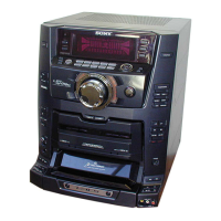
Do you have a question about the Sony HCD-XG900AV and is the answer not in the manual?

Sony HCD-XG900AV Specifications

General IconGeneral
BrandSony
ModelHCD-XG900AV
CategoryStereo System
LanguageEnglish

Summary

Amplifier Specifications

Front Speaker Specifications

Details on DIN power output, Continuous RMS power output, and Music power output for front speakers.

Center Speaker Specifications

Details on DIN power output, Continuous RMS power output, and Music power output for center speakers.

Rear Speaker Specifications

Details on DIN power output, Continuous RMS power output, and Music power output for rear speakers.

Specifications

HCD-XG100AV Specifications

Technical specifications for the HCD-XG100AV, including power output and other details.

Input Specifications

Detailed input specifications including sensitivity and impedance for various input jacks.

Output Specifications

Detailed output specifications including voltage, impedance, and type for various output jacks.

SERVICING NOTES

Optical Pick-up Handling Precautions

Handling precautions for the optical pick-up block to prevent electrostatic breakdown.

Laser Diode Emission Safety

Safety guidelines for checking laser diode emission, observing from a distance.

Laser Diode & Focus Check Procedure

Procedure for checking laser diode and focus search, using 'S curve check'.

Model Identification

Information on identifying models via part numbers on the rear panel.

GENERAL

Front Panel Controls Overview

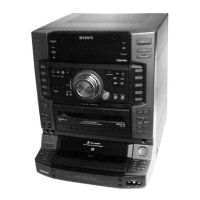
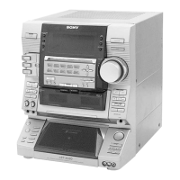
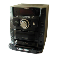
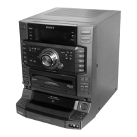
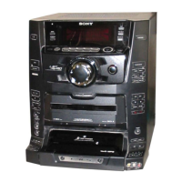
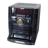
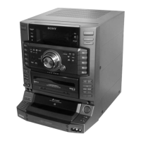
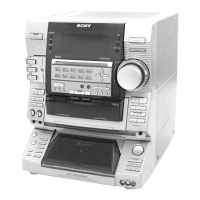
Diagram and labels for front panel controls.

Front Panel Button Descriptions

Explanation of various buttons and their functions on the front panel.

Clock Setting Procedure

Step-by-step guide to set the system clock time.

DISASSEMBLY

Disassembly Flowchart

Step-by-step procedure for disassembling the set.

Case Disassembly

Instructions and diagram for disassembling the main case of the unit.

Front Panel Section Disassembly

Steps and diagram for disassembling the front panel section.

Tape Mechanism Deck Cover & Unit Disassembly

Steps for removing the tape mechanism deck cover and deck.

Main Board (XG100AV) with Fan Disassembly

Procedure for disassembling the main board with the DC fan for XG100AV.

Main Board (XG900AV) Disassembly

Procedure for disassembling the main board for XG900AV.

CD Mechanism Deck Disassembly

Steps for disassembling the CD mechanism deck.

Base Unit Disassembly

Procedure for disassembling the base unit.

Disc Table Installation & Adjustment

Instructions for installing and adjusting the disc table.

TEST MODE

Test Modes Overview

Explanation of various test modes including resets, tuning interval change, and delivery mode.

LED/Indicator & Key Check Mode

Procedure for activating the all-lit mode and key check function.

MECHANICAL ADJUSTMENTS

Mechanical Adjustment Precautions

Important precautions before performing mechanical adjustments.

Torque Measurement Specifications

Table detailing torque values for various tape deck mechanisms.

ELECTRICAL ADJUSTMENTS

Electrical Adjustment Precautions

Precautions for electrical adjustments, emphasizing order and safety.

Deck Section Electrical Adjustments

Overview of adjustments for the deck section, including azimuth, speed, and level.

Head Azimuth Adjustment

Procedure to adjust azimuth for record/playback heads on both decks.

Tape Speed Adjustment Procedure

Procedure to adjust tape speed for Deck B using a frequency counter.

Playback Level Adjustment Procedure

Procedure to adjust playback level for Deck A and Deck B.

Record Bias Adjustment Procedure

Procedure for adjusting record bias for Deck B.

Record Level Adjustment Procedure

Procedure for adjusting record level for Deck B.

CD SECTION

S-Curve Check Procedure

Procedure for checking CD S-curve waveform symmetry and peak level.

E-F Balance (1 Track Jump) Check

Procedure to check E-F balance and DC voltage in 1 track jump mode.

RF Level Check Procedure

Procedure to check RF signal level and waveform clarity for CD playback.

DIAGRAMS

CD Servo Block Diagram

Block diagram illustrating the CD servo system.

Tuner/Tape Deck Block Diagram

Block diagram of the tuner and tape deck sections.

Main Section Block Diagram (1/2)

Part 1 of the block diagram for the main section.

Main Section Block Diagram (2/2)

Part 2 of the block diagram for the main section.

Display/Key Control/Power Supply Block Diagram

Block diagram of display, key control, and power supply.

NOTE FOR PRINTED WIRING BOARDS AND SCHEMATIC DIAGRAMS

Printed Wiring Board Interpretation Notes

Notes on interpreting printed wiring board diagrams, including part indicators.

Schematic Diagram Interpretation Notes

Notes on interpreting schematic diagrams, including component symbols and tolerances.

Circuit Board Locations Diagram

Diagram showing the physical location of various circuit boards within the unit.

PRINTED WIRING BOARD - BD Board

BD Board PWB (Side A)

Printed wiring board layout for the BD board, component side.

BD Board PWB (Side B)

Printed wiring board layout for the BD board, conductor side.

SCHEMATIC DIAGRAM - BD Board

BD Board Schematic

Schematic diagram for the BD board.

PRINTED WIRING BOARDS - CD MOTOR Section

CD Motor PWB

Printed wiring board layout for the CD motor and related boards.

Table Sensor Board PWB

Printed wiring board layout for the table sensor board.

LED Board PWB

Printed wiring board layout for the LED board.

SCHEMATIC DIAGRAM - CD MOTOR Section

CD Motor Schematic

Schematic diagram for the CD motor section.

PRINTED WIRING BOARD - AUDIO Board

AUDIO Board PWB

Printed wiring board layout for the audio board.

SCHEMATIC DIAGRAM - AUDIO Board

AUDIO Board Schematic

Schematic diagram for the audio board.

PRINTED WIRING BOARD - LEAF SW Board

LEAF SW Board PWB

Printed wiring board layout for the leaf SW board.

SCHEMATIC DIAGRAM - LEAF SW Board

LEAF SW Board Schematic

Schematic diagram for the leaf SW board.

SCHEMATIC DIAGRAM - MAIN Board (1/3)

Main Board Schematic (1/3)

Part 1 of the schematic diagram for the main board.

SCHEMATIC DIAGRAM - MAIN Board (2/3)

Main Board Schematic (2/3)

Part 2 of the schematic diagram for the main board.

SCHEMATIC DIAGRAM - MAIN Board (3/3)

Main Board Schematic (3/3)

Part 3 of the schematic diagram for the main board.

PRINTED WIRING BOARD MAIN Board

Main Board PWB

Printed wiring board layout for the main board.

Waveform Diagrams

BD Board Waveforms

Oscilloscope waveforms for BD board tests.

Main Board Waveforms

Oscilloscope waveforms for main board tests.

Panel FL Board Waveforms

Oscilloscope waveforms for Panel FL board tests.

PRINTED WIRING BOARD - PA Board

PA Board PWB

Printed wiring board layout for the PA board.

SCHEMATIC DIAGRAM - PA Board

PA Board Schematic

Schematic diagram for the PA board.

PRINTED WIRING BOARD - SURROUND Board

Surround Board PWB

Printed wiring board layout for the surround board.

SCHEMATIC DIAGRAM - SURROUND Board

Surround Board Schematic

Schematic diagram for the surround board.

PRINTED WIRING BOARDS - MIC/FRONT INPUT/HEADPHONES Boards

MIC Board PWB

Printed wiring board layout for the MIC board.

Front Input Board PWB

Printed wiring board layout for the front input board.

Headphones Board PWB

Printed wiring board layout for the headphones board.

SCHEMATIC DIAGRAM - MIC/FRONT INPUT/HEADPHONES Boards

MIC Board Schematic

Schematic diagram for the MIC board.

Front Input Board Schematic

Schematic diagram for the front input board.

Headphones Board Schematic

Schematic diagram for the headphones board.

PRINTED WIRING BOARD - PANEL FL Board

Panel FL Board PWB

Printed wiring board layout for the PANEL FL board.

SCHEMATIC DIAGRAM - PANEL FL Board

Panel FL Board Schematic

Schematic diagram for the PANEL FL board.

PRINTED WIRING BOARDS - PANEL VR/ILLUMINATION Boards

Panel VR/Illumination Boards PWB

Printed wiring board layouts for PANEL VR and ILLUMINATION boards.

SCHEMATIC DIAGRAM - PANEL VR/ILLUMINATION Boards

Panel VR/Illumination Boards Schematic

Schematic diagrams for PANEL VR and ILLUMINATION boards.

PRINTED WIRING BOARDS - TC-A/TC-B/CD-L/CD-R (1)/CD-R (2) Boards

TC-A Board PWB

Printed wiring board layout for the TC-A board.

TC-B Board PWB

Printed wiring board layout for the TC-B board.

CD-L Board PWB

Printed wiring board layout for the CD-L board.

CD-R (1) Board PWB

Printed wiring board layout for the CD-R (1) board.

CD-R (2) Board PWB

Printed wiring board layout for the CD-R (2) board.

SCHEMATIC DIAGRAM - TC-A/TC-B/CD-L/CD-R (1)/CD-R (2) Boards

TC-A Board Schematic

Schematic diagram for the TC-A board.

TC-B Board Schematic

Schematic diagram for the TC-B board.

CD-L Board Schematic

Schematic diagram for the CD-L board.

CD-R (1) Board Schematic

Schematic diagram for the CD-R (1) board.

CD-R (2) Board Schematic

Schematic diagram for the CD-R (2) board.

PRINTED WIRING BOARDS - TRANSFORMER Section

Transformer Section PWB

Printed wiring board layouts for the transformer section.

SCHEMATIC DIAGRAM - TRANSFORMER Section

Transformer Section Schematic

Schematic diagram for the transformer section.

IC Block Diagrams - BD Board

BD Board IC Block Diagrams

IC block diagrams for the BD board.

IC Diagrams

IC103 CXA2568M-T6 Block Diagram

Block diagram for IC103 CXA2568M-T6.

CD Motor IC201 TA8409S Block Diagram

Block diagram for IC201 TA8409S on the CD motor board.

IC Diagrams

Audio Board IC101 M62493FP Block Diagram

Block diagram for IC101 M62493FP on the audio board.

IC Diagrams

IC191 BA7615N Block Diagram

Block diagram for IC191 BA7615N.

IC201 M62464FP Block Diagram

Block diagram for IC201 M62464FP.

IC Diagrams

Panel FL Board IC602 BA3830F Block Diagram

Block diagram for IC602 BA3830F on the Panel FL board.

Panel VR Board IC701 NJU3716L Block Diagram

Block diagram for IC701 NJU3716L on the Panel VR board.

IC PIN FUNCTION DESCRIPTION

Main Board IC501 M30622MAA-A92FP Pin Functions

Detailed pin function description for IC501 on the main board.

IC Pin Function Descriptions (Continued)

Continued pin function descriptions for IC501, covering more pins.

IC Pin Function Descriptions (Continued)

Further pin function descriptions for IC501, covering remaining pins.

Panel FL Board IC601 Pin Functions

Pin function description for IC601 on the Panel FL board.

Panel FL Board IC601 Pin Functions (Continued)

Continued pin function descriptions for IC601.

Panel VR Board IC701 Pin Functions

Pin function description for IC701 on the Panel VR board.

EXPLODED VIEWS

Exploded Views Notes

Notes regarding parts identification, stocking, and markings in exploded views.

Case & Back Panel Exploded View

Exploded view and parts list for the case and back panel.

Front Panel Section-1 Exploded View

Exploded view and parts list for the front panel section (part 1).

Front Panel Section-2 Exploded View

Exploded view and parts list for the front panel section (part 2).

Chassis Section Exploded View

Exploded view and parts list for the chassis section.

CD Mechanism Deck Exploded View

Exploded view and parts list for the CD mechanism deck.

Base Unit Section Exploded View

Exploded view and parts list for the base unit section.

Tape Mechanism Deck Section-1 Exploded View

Exploded view and parts list for the tape mechanism deck section (part 1).

Tape Mechanism Deck Section-2 Exploded View

Exploded view and parts list for the tape mechanism deck section (part 2).

ELECTRICAL PARTS LIST

AUDIO Board Parts List

List of electrical components for the Audio board, including ICs, Capacitors, Coils, Transistors, Resistors.

Electrical Parts List - Components

Continuation of the electrical parts list, detailing components for various boards.

Hardware & Accessories Lists

Lists of hardware, accessories, and packing materials.

REVISION HISTORY

Revision History Details

Records of revisions made to the service manual.

Related product manuals