— 3 —
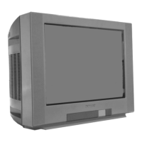
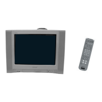
KV-21FA210
TABLE OF CONTENTS
SECTION TITLE PAGE
Specications ............................................................................................................................................................................. 4
Warnings and Cautions .............................................................................................................................................................. 5
Safety Check-Out ....................................................................................................................................................................... 6
Self-Diagnostic Function............................................................................................................................................................. 7
SECTION 1: DISASSEMBLY............................................................................................................................................................. 9
1-1. Rear Cover Removal.......................................................................................................................................................... 9
1-2. Chassis Assembly Removal............................................................................................................................................... 9
1-3. Service Position ................................................................................................................................................................. 9
1-4. Picture Tube Removal...................................................................................................................................................... 10
Anode Cap Removal Procedure....................................................................................................................................... 10
SECTION 2: SET-UP ADJUSTMENTS.............................................................................................................................................11
2-1. Beam Landing...................................................................................................................................................................11
2-2. Convergence.................................................................................................................................................................... 12
2-3. Focus ............................................................................................................................................................................... 13
2-4. Screen (G2)...................................................................................................................................................................... 14
2-5. Method of Setting the Service Adjustment Mode ............................................................................................................. 14
2-6. White Balance Adjustments ............................................................................................................................................. 14
SECTION 3: SAFETY RELATED ADJUSTMENTS......................................................................................................................... 15
3-1.
X
R565 Conrmation Method (HV Hold-Down Conrmation) and Readjustments ........................................................ 15
3-2. B+ Voltage Conrmation and Adjustment ........................................................................................................................ 15
SECTION 4: CIRCUIT ADJUSTMENTS .......................................................................................................................................... 17
4-1. Setting the Service Adjustment Mode .............................................................................................................................. 17
4-2. Memory Write Conrmation Method ................................................................................................................................ 17
4-3. Remote Adjustment Buttons and IndicatorS .................................................................................................................... 17
4-4. ID Map Table .................................................................................................................................................................... 26
4-5. A Board Adjustments........................................................................................................................................................ 26
SECTION 5: DIAGRAMS................................................................................................................................................................. 29
5-1. Circuit Boards Location.................................................................................................................................................... 29
5-2. Printed Wiring Board and Schematic Diagram Information.............................................................................................. 29
5.3 Block Diagram and Schematics ....................................................................................................................................... 30
A Board Schematic Diagram ............................................................................................................................................ 31
M3 Board Schematic Diagram ......................................................................................................................................... 36
HR Board Schematic Diagram ......................................................................................................................................... 38
CV Board Schematic Diagram ......................................................................................................................................... 39
K Board Schematic Diagram............................................................................................................................................ 41
KB Board Schematic Diagram ......................................................................................................................................... 41
5-4. Semiconductors ............................................................................................................................................................... 42
SECTION 6: EXPLODED VIEWS.................................................................................................................................................... 43
6-1. Picture Tube..................................................................................................................................................................... 43
6-2. Chassis ............................................................................................................................................................................ 44
SECTION 7: ELECTRICAL PARTS LIST........................................................................................................................................ 45