MC-S50
1414
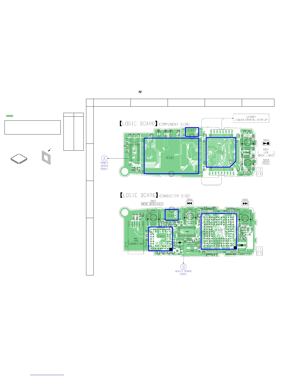
Note on Printed Wiring Board:
• Y : parts extracted from the conductor side.
•
f
: internal component.
• : Pattern from the side which enables seeing.
(The other layers' patterns are not indicated.)
Caution:
Pattern face side: Parts on the pattern face side seen from
(Conductor Side) the pattern face are indicated.
Parts face side: Parts on the parts face side seen from
(Component Side) the parts face are indicated.
4-2. NOTE FOR PRINTED WIRING BOARDS
AND SCHEMATIC DIAGRAMS
• AUDIO, LOGIC and POWER boards are multi-layer printed
board.
However, the patterns of intermediate-layer have not been in-
cluded in this diagrams.
Note on Schematic Diagram:
• All capacitors are in µF unless otherwise noted. pF: µµF
50 WV or less are not indicated except for electrolytics
and tantalums.
• All resistors are in Ω and
1
/
4
W or less unless otherwise
specified.
• % : indicates tolerance.
•
f
: internal component.
• C : panel designation.
• A : B+ Line.
• Power voltage is dc 1.5 V and fed with regulated dc power
supply from battery terminal.
• Voltages and waveforms are dc with respect to ground in
playback mode.
no mark : PLAYBACK
∗
: Impossible to measure
• Voltages are taken with a VOM (Input impedance 10 MΩ).
Voltage variations may be noted due to normal produc-
tion tolerances.
• Waveforms are taken with a oscilloscope.
Voltage variations may be noted due to normal produc-
tion tolerances.
• Circled numbers refer to waveforms.
• Signal path.
F : PLAYBACK
* The voltage and waveform of CSP (chip size package)
cannot be measured, because its lead layout is different
form that of conventional IC.
* Lead Layouts (IC601 and IC901)
surfac