22
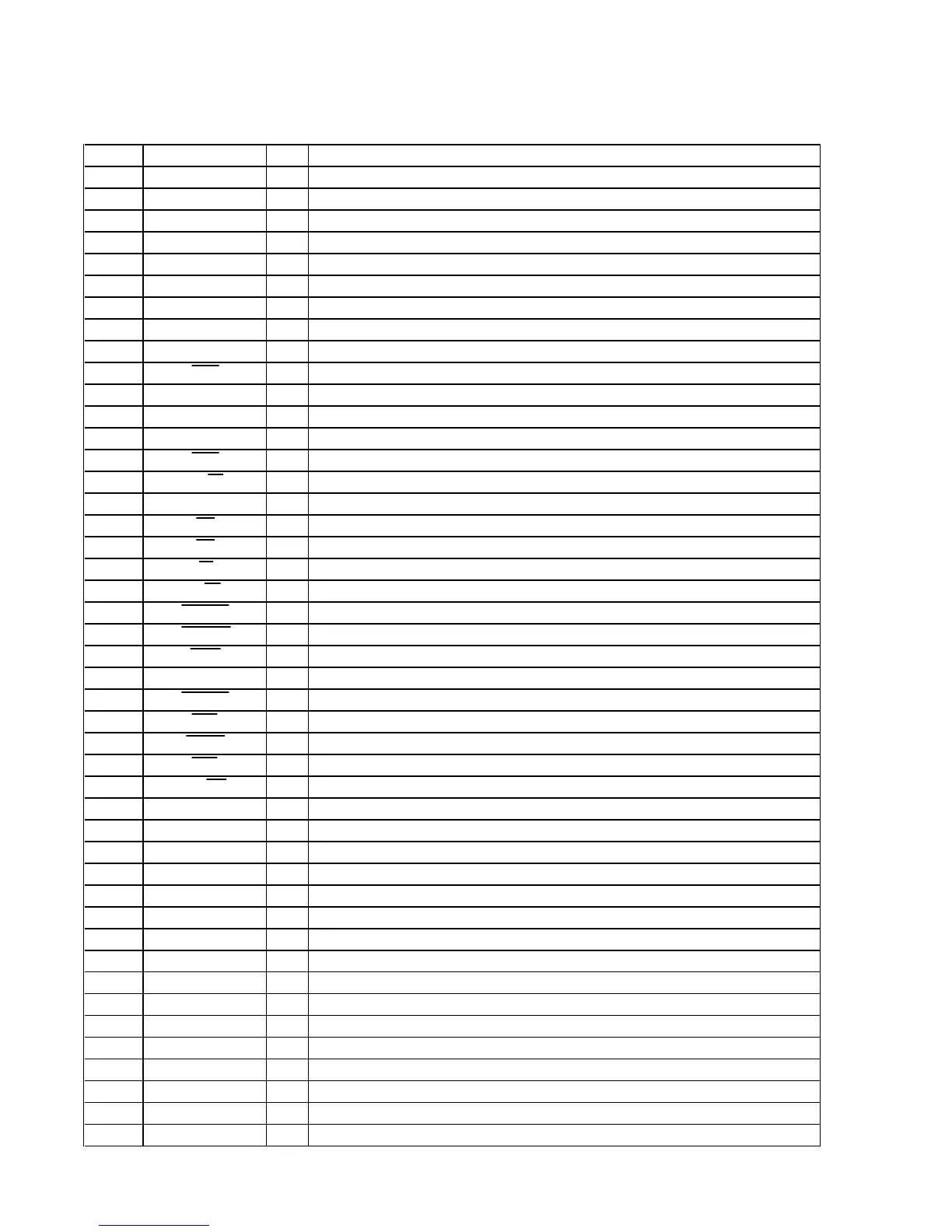
MC-S50
4-9. IC PIN FUNCTION DESCRIPTION
• LOGIC BOARD IC601 TMS320DA150GGU120 (DIGITAL SIGNAL PROCESSOR) (Not supplied part)
Pin No. Pin Name I/O
Description
1CVSS—
Ground terminal
2A22—
Address signal terminal Not used (open)
3CVSS—
Ground terminal
4 DVDD —
Power supply terminal (+3.2V)
5A10—
Address signal terminal Not used (open)
6HD7
O Muting control signal output terminal “L”: muting
7 to 10 A11 to A14
I Address signal input terminal Not used (open)
11 A15
O Read/write signal output to the 2 to 4 decoder (IC604)
12 CVDD
— Power supply terminal (+1.5V)
13 HAS
I Address strobe signal input terminal Not used (fixed at “H”)
14 DVSS
— Ground terminal
15 CVSS —
Ground terminal
16 CVDD
— Power supply terminal (+1.5V)
17 HCS
I Chip select signal input terminal Not used (fixed at “H”)
18 HR/W
I Read/write signal input terminal Not used (fixed at “H”)
19 READY
I Data ready signal input terminal Not used (fixed at “H”)
20 PS
O Program space select signal output terminal Not used (open)
21 DS
O Data space select signal output terminal Not used (open)
22 IS
O I/O space select signal output to the USB controller (IC901)
23 R/W
O Read/write signal output to the 2 to 4 decoder (IC604)
24 MSTRB
O Memory strobe signal output terminal Not used (open)
25 IOSTRB
O I/O strobe signal output to the 2 to 4 decoder (IC604)
26 MSC O
Microstate complete signal output terminal Not used (open)
27 XF O
External flag signal output terminal Not used (open)
28 HOLDA O
Hold acknowledge signal output terminal Not used (open)
29 IAQ O
Instruction acquisition signal output terminal Not used (open)
30 HOLD I
Hold signal input terminal Not used (fixed at “H”)
31 BIO I
Branch control signal input terminal Not used (fixed at “H”)
32 MP/MC I
Mode select signal input terminal Not used (fixed at “L”)
33 DVDD —
Power supply terminal (+3.2V)
34 CVSS
— Ground terminal
35 BDR1
I Serial data receive signal input terminal Not used (fixed at “H”)
36 BFSR1
I Frame synchronization pulse signal input terminal Not used (fixed at “H”)
37 CVSS
— Ground terminal
38 BCLKR1
O Serial clock signal output to the CPU (IC801)
39 HCNTL0
I Control signal input terminal Not used (fixed at “H”)
40 DVSS
— Ground terminal
41, 42 BCLKR0, BCLKR2
I Data receive clock input terminal Not used (fixed at “H”)
43, 44 BFSR0, BFSR2
I Frame synchronization pulse signal input terminal Not used (fixed at “H”)
45 BDR0
I Serial data receive signal input from the flash ROM (IC602)
46 HCNTL1
I Control signal input terminal Not used (fixed at “H”)
47 BDR2
I Serial data receive signal input from the EEPROM (IC603) and CPU (IC801)
48 BCLKX0
O Serial clock signal output to the D/A converter (IC302)
49 BCLKX2
O Serial clock signal output to the EEPROM (IC603) and CPU (IC801)
50 CVSS
— Ground terminal