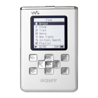
22
NW-E002F/E003F/E005F
Pin No. Pin Name I/O Description
95 DVS — Ground terminal
96 DVDIO2 — Power supply terminal
97 DVS — Ground terminal
98 MSBS/INT0/GPIOE0 O MS_BS (Not used)
99 MSSCLK O MS_SCLK (Not used)
100 MSDIO0/GPIOE1 O MS control (Not used)
101 MSDIO1/GPIOE2 I Battery charge control signal input
102 MSDIO2/GPIOE3 O USB power signal input
103 MSDIO3/GPIOE4 O Battery charge control signal output
104 MSINS/GPIOE5 I MS control (Not used)
105 MCSEL I Oscillator select (Connected to +2.8V)
106 CBIAS — HP Amp com BIAS
107 CCOM — HP Amp com out
108 HPREF — HP Amp Reference (Pull down)
109 CSOFT — HP Amp TC
110 TESTAUD — For TEST (Not used)
111 DGND — Ground terminal
112 DVDD — Power supply terminal
113 ARST O Reset signal output for FLASH ROM and SRAM
114 AVDOSC1 — Power supply terminal
115 EXTAL I Oscillator connection terminal for main oscillation (45MHz)
116 XTAL O Oscillator connection terminal for main oscillation (45MHz)
117 AVSOSC — Ground terminal
118 TEX I Oscillator connection terminal for sub oscillation (12MHz)
119 TX O Oscillator connection terminal for sub oscillation (12MHz)
120 AVDOSC2 — Power supply terminal
121 AVSPLL — Ground terminal
122 AVDPLL — Power supply terminal
123 AVDUSB — Power supply terminal
124 AVSUSB — Ground terminal
125 DP I/O USB DATA + signal
126 DM I/O USB DATA – signal
127 VBUS/GPIOD0 I USB power signal input
128 TXD0/GPIOI0 O UART0 (Not used)
129 RXD0/GPIOI1 I UART0 (Connected to +2.8V)
130 TXD1/GPIOJ1 O UART1 out
131 RXD1/GPIOJ1 I UART1 in
132 SI0/GPIOG1 I Tuner status input
133 SO0/GPIOG0 O Serial data signal output for tuner
134 SCK0 O Serial clock signal output for tuner
135 SCS0/GPIOG2 I/O Serial latch signal for tuner
136 SI1/GPIOH1 O Serial data signal output for IC801
137 SO1/GPIOH0 I Serial data signal input for IC801
138 SCK1 O Serial clock signal output for IC801
139 SCS1/GPIOH2 I RTC SCLK (Not used)
140 DVS — Ground terminal
141 DVDIO1 — Power supply terminal
142 DVDIO1 — Power supply terminal
143 DVS — Ground terminal