8
NW-E99
SECTION 4
DIAGRAMS
Note on Schematic Diagram:
• All capacitors are in µF unless otherwise noted. (p: pF) 50 WV or
less are not indicated except for electrolytics and tantalums.
• All resistors are in Ω and
1
/
4
W or less unless otherwise specified.
•%: indicates tolerance.
• C : panel designation.
• : B+ Line.
•Power voltage is dc 1.5 V and fed with regulated dc power supply
from battery terminal.
•Voltages and waveforms are dc with respect to ground under no-
signal (detuned) conditions.
no mark : PLAY
•Voltages are taken with a VOM (Input impedance 10 MΩ).
Voltage variations may be noted due to normal production toler-
ances.
•Waveforms are taken with a oscilloscope.
Voltage variations may be noted due to normal production toler-
ances.
• Circled numbers refer to waveforms.
• Signal path.
F : PLAY
a : DIGITAL OUT
k : DIGITAL IN
Note on Printed Wiring Board
• X : parts extracted from the component side.
• Y : parts extracted from the conductor side.
• : Pattern from the side which enables seeing.
•: Through hole.
Caution:
Pattern face side: Parts on the pattern face side seen from
(Side A) the pattern face are indicated.
Parts face side: Parts on the parts face side seen from
(Side B) the parts face are indicated.
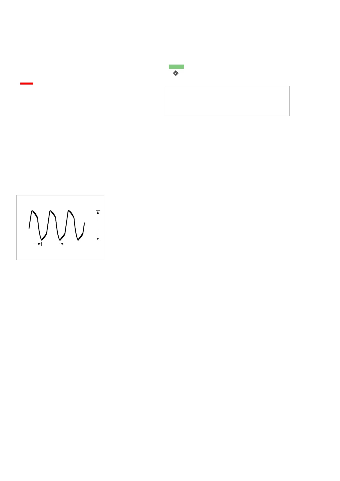
• Waveform
1
IC700 8 (OSCOUT)
0.5 V/div, 10
µ
sec/div
1.1 Vp-p
31.25
µ
sec