65
SCD-XB770
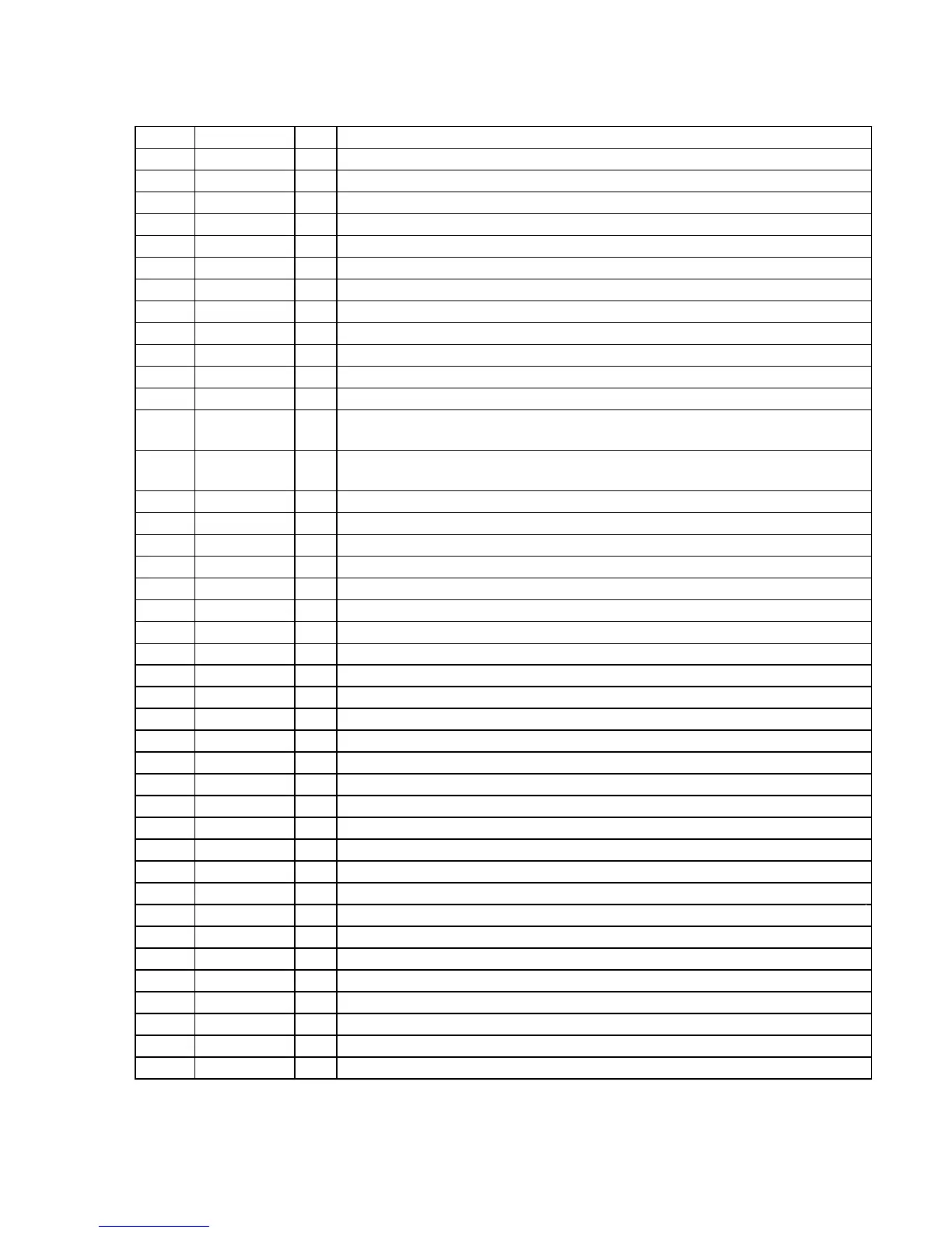
Pin No. Pin Name I/O Description
57 VDD —
Power supply terminal (+3.3V) (digital system)
58 DSAR O
DSD data (front R-ch) output to the digital filter (IC301)
59 GND —
Ground terminal (digital system)
60 DSALS O
DSD data (surround L-ch) output to the digital filter (IC302)
61 GND —
Ground terminal (digital system)
62 DSARS O
DSD data (surround R-ch) output to the digital filter (IC302)
63 VDD —
Power supply terminal (+3.3V) (digital system)
64 DSAC O
DSD data (center) output to the digital filter (IC303)
65 GND —
Ground terminal (digital system)
66 DSASW O
DSD data (sub woofer) output to the digital filter (IC303)
67 GND —
Ground terminal (digital system)
68 PHREFI I
Phase reference signal input terminal for DSD output phase modulation
69 PHREFO O
Phase reference signal output for DSD output phase modulation to the digital filter (IC301 to
IC303)
70 BCKASL I
Input/output selection signal input terminal of bit clock signal (2.8224 MHz) for DSD data output
“L”: input (slave), “H”: output (master) (fixed at “L” in this set)
71 BCKAO O
Bit clock signal (2.8224 MHz) output terminal for DSD data output Not used (open)
72 BCKAI I
Bit clock signal (2.8224 MHz) input terminal for DSD data output Not used
73, 74 TESTO O
Output terminal for the test Not used
75 VDD —
Power supply terminal (+3.3V) (digital system)
76 GND —
Ground terminal (digital system)
77 TESTI I
Input terminal for the test (normally: fixed at “L”)
78 TESTI I
Input terminal for the test Not used
79
XSBSL2
I
HD mode selection signal input from the I/O expander (IC902)
80, 81 TESTI I
Input terminal for the test Not used
82
XABSL1
I
HD mode selection signal input from the I/O expander (IC902)
83, 84 TESTO O
Output terminal for the test Not used
85 DVCKI I
11.2896 MHz clock signal input terminal
86 TESTI I
Input terminal for the test Not used
87 GND —
Ground terminal (digital system)
88 MCKI I
Master clock signal (33.8688 MHz) input terminal
89 VDD —
Power supply terminal (+3.3V) (digital system)
90 LRCK O
L/R sampling clock signal (44.1kHz) output to the digital filter (IC301 to IC303)
91 CDDATAR O
Serial data output terminal Not used (open)
92 CDDATAL O
Serial data output to the digital filter (IC301)
93
CDDATASL
I
CD mode selection signal input from the I/O expander (IC902)
94 BCKI I
Bit clock signal (2.8224 MHz) input from the CXD3068Q (IC509)
95 LRCKI I
L/R sampling clock signal (44.1 kHz) input from the CXD3068Q (IC509)
96 CDDATAI I
Serial data input from the CXD3068Q (IC509)
97 TESTI I
Input terminal for the test (normally: fixed at “L”)
98 SMUTE I
Muting on/off signal input from the CPU (IC901) “H”: muting on
99 XRST I
Reset signal input from the I/O expander (IC902) “L”: reset
100 GND —
Ground terminal (digital system)


 To Next Page