– 5 –
– 6 –
SECTION 3
DIAGRAMS
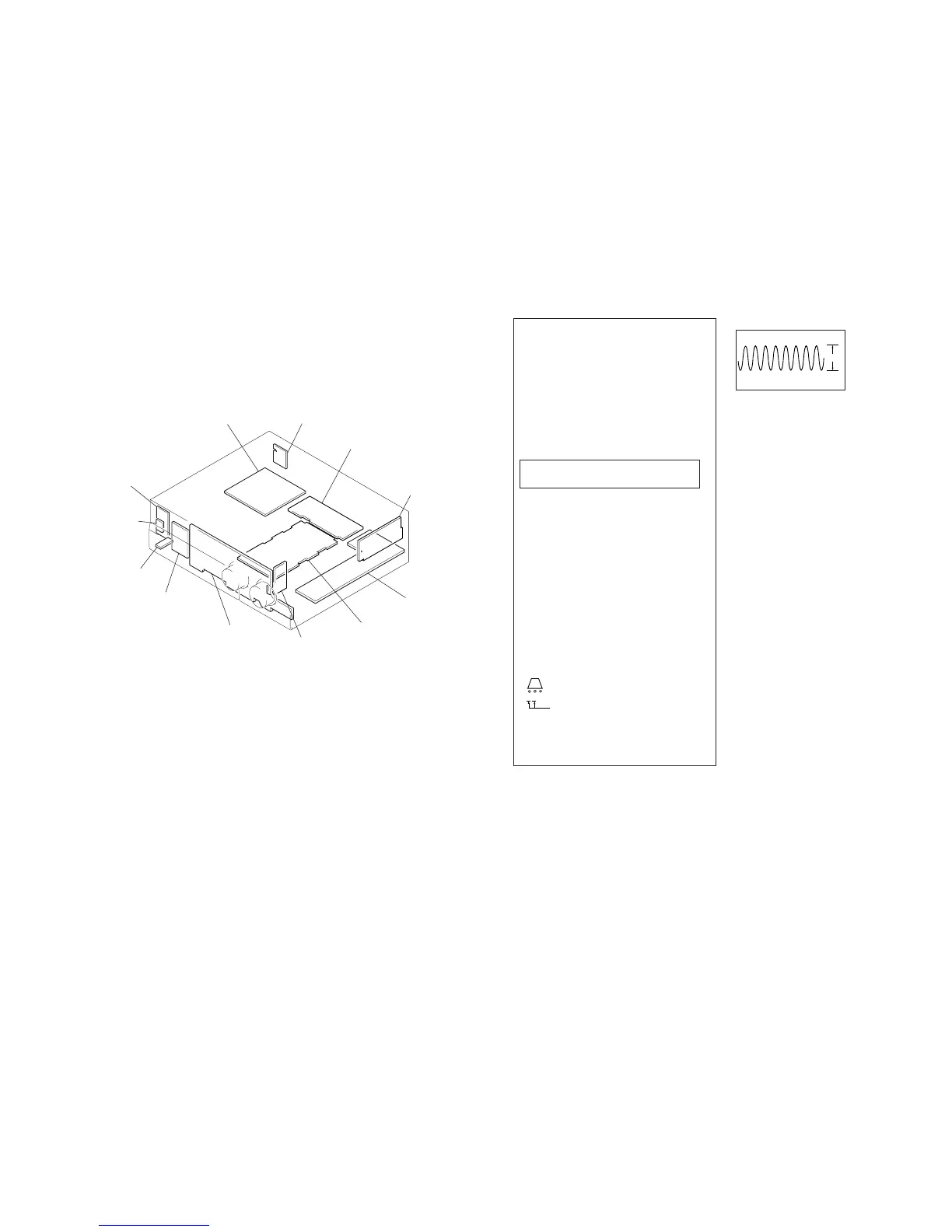
3-1. CIRCUIT BOARDS LOCATION
THIS NOTE IS COMMON FOR PRINTED WIRING
BOARDS AND SCHEMATIC DIAGRAMS.
(In addition to this, the necessary note is printed
in each block.)
For schematic diagrams.
Note:
• All capacitors are in µF unless otherwise noted. pF: µµF
50 WV or less are not indicated except for electrolytics
and tantalums.
• All resistors are in Ω and
1
/
4
W or less unless otherwise
specified.
•
¢
: internal component.
• 2 : nonflammable resistor.
• 5 : fusible resistor.
• C : panel designation.
For printed wiring boards.
Note:
• X : parts extracted from the component side.
• Y : parts extracted from the conductor side.
• b : Pattern from the side which enables seeing.
• U : B+ Line.
• V : B– Line.
• H : adjustment for repair.
• Voltages and waveforms are dc with respect to ground
under no-signal (detuned) conditions.
no mark : POWER ON
• Voltages are taken with a VOM (Input impedance 10 MΩ).
Voltage variations may be noted due to normal produc-
tion tolerances.
• Waveforms are taken with a oscilloscope.
Voltage variations may be noted due to normal produc-
tion tolerances.
• Circled numbers refer to waveforms.
• Signal path.
F : TUNER
WAVEFORM
1
IC902 1 XOUT
Note: The components identified by mark ! or dotted line
with mark ! are critical for safety.
Replace only with part number specified.
• Indication of transistor
C
These are omitted
EB
4MHz
3.8Vp-p
PANEL board
INPUT board
MAIN board
SP-TM board
PHONO boar
 Loading...