TA-FE370/FE570
1414
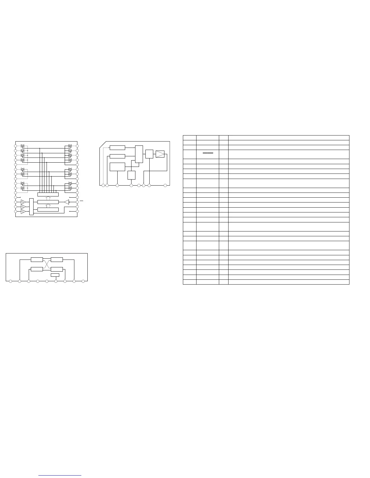
• IC Block Diagrams
– MAIN Board –
IC101 LC7821
IC601 µPC1237HA
1
2
3
4
5
6
7
8
9
10
11
12
13
14
15
30
29
28
27
26
25
24
23
22
21
20
19
18
17
16
CONTROL
LATCH
SHIFT RESISTER
LEVEL SHIFT
CL
DI
CE
VEE
L COM3
L7
L COM2
L5
L4
L2
VSS
S
RES
VDD
R COM3
R8
R7
R COM2
R6
R4
R2
R5
R COM1
R3
R1
L3
L1
L COM1
L6
L8
BUFFER
1 2 3
4 5 6 7 8
OVER LOAD DET
F/F
OFFSET DET
LATCH/
AUTORESET
V
CC ON
MUTE
AC OFF
DET
OVER LOAD DET
OFFSET DET
AUTO RESET
AC OFF DET
GND
RELAY DRIVE
VCC ON MUTE
VCC
– CONTROL Board –
IC802 BA6208
1 2 3 4 5 6 7
8
9
NC
OUTPUT 2
Vcc
GND
NC
INPUT 2
INPUT 1
NC
MOTOR
DRIVE
MOTOR
DRIVE
REG
SWITCH
SWITCH
OUTPUT1
4-8. IC PIN FUNCTION DESCRIPTION
• CONTROL BOARD IC801 TMP47C103N-JP47 (FUNCTION SWITCH CONTROL, LED DRIVER)
Pin No. Pin Name I/O Description
1 XOUT O Main system clock output terminal (4 MHz)
2 XIN I Main system clock input terminal (4 MHz)
3 RESET I
System reset signal input terminal “L”: reset
For several hundreds msec. after the power supply rises, “L” is input, then it changes to “H”
4 PMD I Setting terminal for the model (Fixed at “H” in this set)
5 VOL+ O Motor drive signal output to the volume motor drive (IC802) (volume up direction)
6VOL– O Motor drive signal output to the volume motor drive (IC802) (volume down direction)
7 to 9 SW0 to SW2 I Rotary switch input of the INPUT SELECTOR (S801)
10 EON I
Detection signal input of the enhanced other networks (EON) (Used for the TA-FE570)
TA-FE370: Not used (fixed at “H”)
11 PHONO O LED drive signal output of the PHONO LED (D808) “L”: LED on
12 TUNER O LED drive signal output of the TUNER LED (D809) “L”: LED on
13 CD O LED drive signal output of the CD LED (D810) “L”: LED on
14 GND — Ground terminal
15 AUX O LED drive signal output of the AUX LED (D811) “L”: LED on
16 TAPE2 O LED drive signal output of the TAPE2/MD LED (D812) “L”: LED on
17 TAPE1 O LED drive signal output of the TAPE1/DAT LED (D813) “L”: LED on
18 MON O
Tape monitor on/off control signal output terminal “L”: tape monitor on
(Used for the TA-FE570) TA-FE370: Not used (pull up)
19 PRY O Power on/off relay drive signal output “L”: power on, “H”: standby mode
20 PKY I POWER switch (S1) input terminal “H”: power on
21 MON I
TAPE1 MONITOR switch (S802) input terminal “H” input when key pressing
(Used for the TA-FE570) TA-FE370: Not used (fixed at “L”)
22 SIRCS I Sircs signal input from the remote control receiver (IC803)
23 MUTE O Audio line muting on/off control signal output “H”: muting on
24 SCE O Chip enable signal output to the function switch (IC101)
25 SDT O Serial data output to the function switch (IC101)
26 SCK O Serial data transfer clock signal output to the function switch (IC101)
27 STOP I Detection signal input of the AC input
28 +3V — Power supply terminal (+3V)