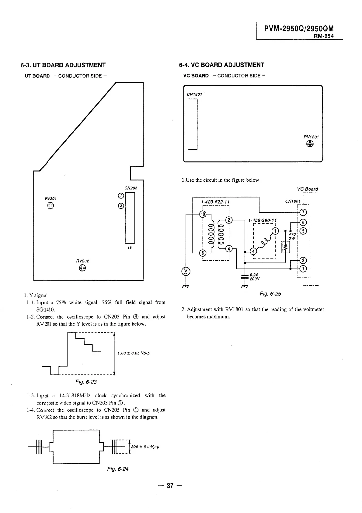
6-3. UT BOARD ADJUSTMENT
UT BOARD - CONDUCTOR SIDE -
RV201
©
RV202
©
1. Y signal
0
0
CN205
18
1-1. Input a 75% white signal, 75% full field signal from
SG141O.
1-2. Connect the oscilloscope to CN2O5 Pin ® and adjust
RV201 so that the Y level is as in the figure below.
1.60 ± 0.05 Vp-p
Fig. 6-23
1-3. Input a 14.31818MHz clock synchronized with the
composite video signal to CN2O3 Pin CD.
1-4. Connect the oscilloscope to CN2O5 Pin CD and adjust
RV202 so that the burst level is as shown in the diagram.
1111 ~,________,~ ll[}w mVpp
Fig. 6-24
PVM-2950Q/2950QM
6-4. VC BOARD ADJUSTMENT
VC BOARD - CONDUCTOR SIDE -
CN1801
-
I .Use the circuit in the figure below
. ·-·-·--'
0.24
I200V
Fig. 6-25
RM-854
RV1801
©
VC Board
2. Adjustment with RV18O1 so that the reading of the voltmeter
becomes maximum.
- 37 -
 Loading...