1212
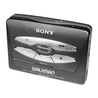
WM-EX422
Note on Schematic Diagram
• All capacitors are in µF unless otherwise noted. pF: µµF 50
WV or less are not indicated except for electrolytics and
tantalums.
• All resistors are in Ω and
1
/
4
W or less unless otherwise speci-
fied.
• C : panel designation.
• : B+ Line.
• H : adjustment for repair.
• Power voltage is dc 1.5V and fed with regulated dc power
supply from battery terminal.
•Voltages and waveforms are dc with respect to ground under
no-signal (detuned) conditions.
• no mark : PLAY
•Voltages are taken with a VOM (Input impedance 10 MΩ).
Voltage variations may be noted due to normal production
tolerances.
•Waveforms are taken with a oscilloscope.
Voltage variations may be noted due to normal production
tolerances.
• Circled numbers refer to waveforms.
• Signal path.
E : PB
Note on Printed Wiring Board
• X : parts extracted from the component side.
• a : Through hole.
• : Pattern from the side which enables seeing.
(The other layers' patterns are not indicated.)
Caution:
Pattern face side: Parts on the pattern face side seen from the
(Side B) pattern face are indicated.
Parts face side: Parts on the parts face side seen from the
(Side A) parts face are indicated.
z
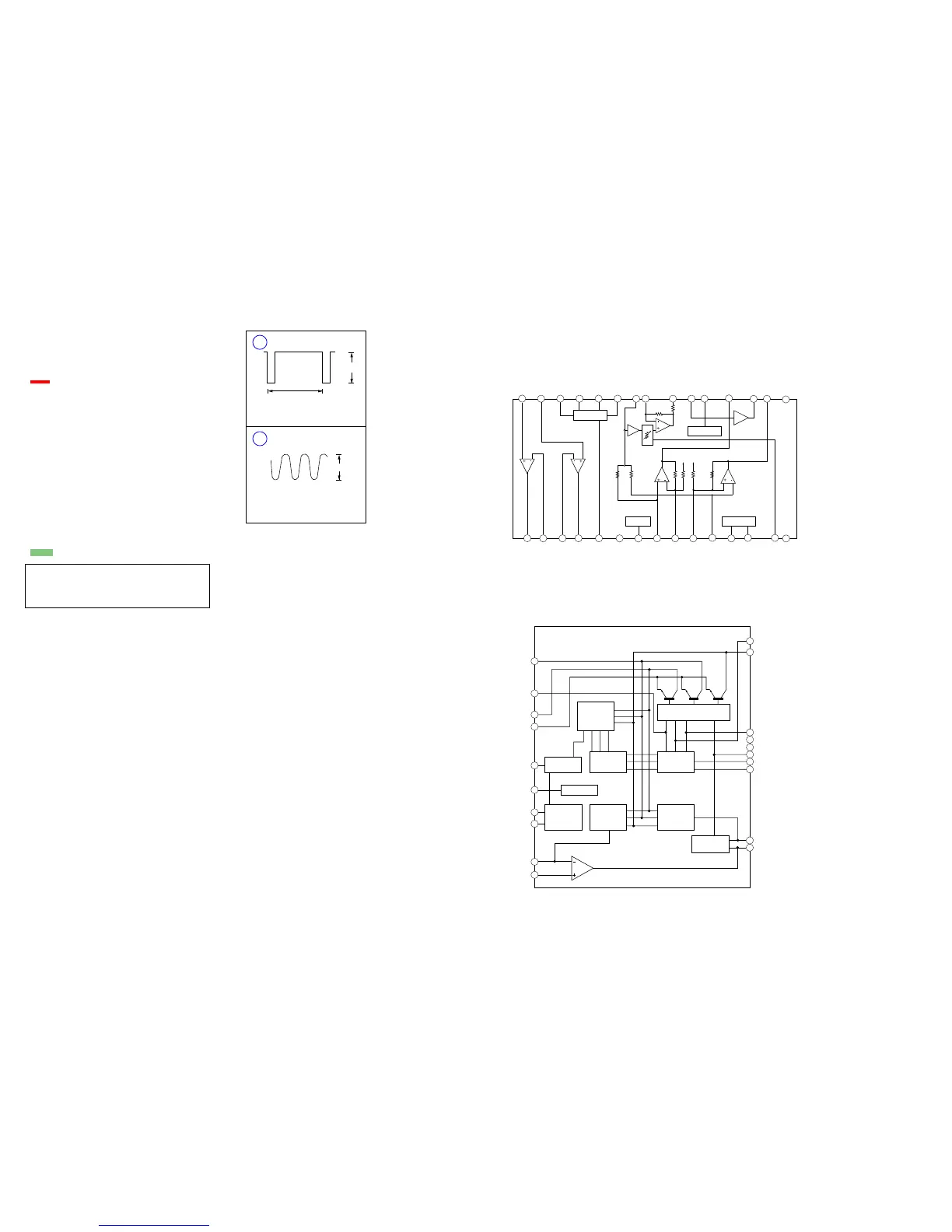
Waveforms
1
IC701 9
VOLT/DIV : 1V AC
TIME/DIV : 20msec
PHOTO CTRL
1.0 Vp-
 Loading...