– 12 –
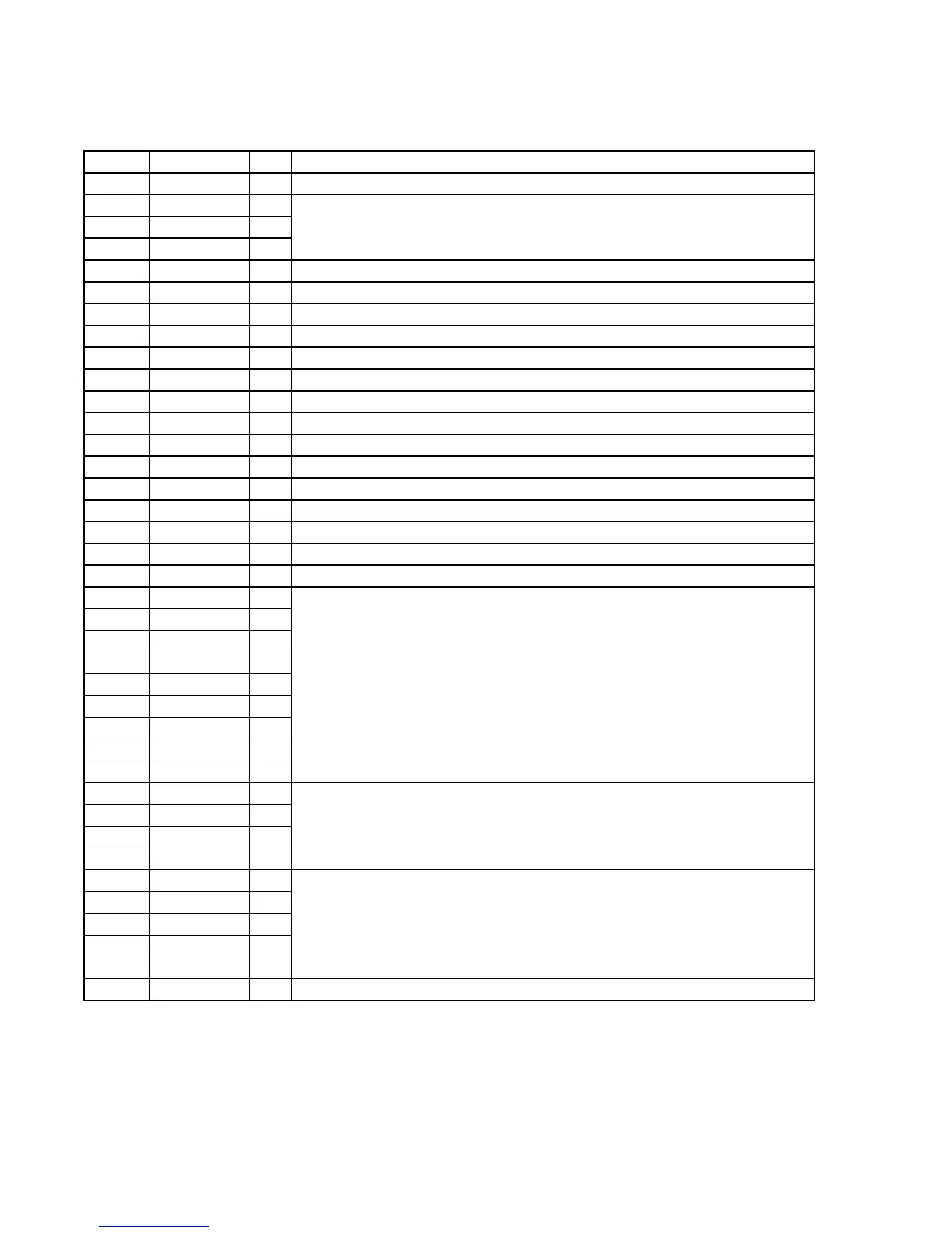
5-1. IC PIN FUNCTION DESCRIPTION
SECTION 5
DIAGRAMS
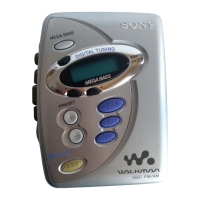
• MAIN BOARD IC401 µPD17015GS-545-GJG-E1 (SYSTEM CONTROLLER, LCD DRIVER)
Pin No. Pin Name I/O Function
1 KEYIN3 I
Key return signal input terminal
2 KEYOUT1 O
3 KEYOUT2 O
Key strobe signal output terminal
4 KEYOUT3 O
5 MUTE O
Muting on/off control signal output to the LA4582CM (IC301) “L”: muting on
6 BEEP/INIT O
Buzzer sound drive signal output terminal
7SDI
Station detector detect signal input from the TA2111F (IC1) SD is present at input of “L”
8 TAPEON I
Tape system power on/off monitor input terminal “H”: tape on
9 RADIOON O
Radio system power supply on/off control signal output “H”: radio on
10 BAND O
Band select signal output to the TA2111F (IC1) “H”: FM, “L”: AM (MW)
11 CE I
Power failure detection signal input terminal (fixed at “H”)
12 XOUT O
System clock output terminal (75 kHz)
13 XIN I
System clock input terminal (75 kHz)
14 VDD —
Power supply terminal (+3V)
15 GND —
Ground terminal
16 EO O
PLL error signal output terminal
17 VREG —
Power supply terminal (connected to the coupling capacitor)
18 VCOFM I
FM VCO input terminal
19 VCOAM I
AM (MW) VCO input terminal
20 LCD8 O
21 LCD7 O
22 LCD6 O
23 LCD5 O
24 LCD4 O
Segment drive signal output to the liquid crystal display (LCD401)
25 LCD3 O
26 LCD2 O
27 LCD1 O
28 LCD0 O
29 COM3 O
30 COM2 O
31 COM1 O
32 COM0 O
33 VLCD1 —
34 CAP1 —
35 CAP0 —
36 VLCD0 —
37 KEYIN1 I
Key return signal input terminal
38 KEYIN2 I
Key return signal input terminal
Terminal for doubler circuit capacitor connection to develop liquid crystal display drive
voltage
Common drive signal output to the liquid crystal display (LCD401)
 Loading...