– 22 –
Note on Schematic Diagram:
• All capacitors are in µF unless otherwise noted. pF: µµF
50 WV or less are not indicated except for electrolytics
and tantalums.
• All resistors are in Ω and
1
/
4
W or less unless otherwise
specified.
•
¢
: internal component.
• C : panel designation.
• U : B+ Line.
• Power voltage is dc 3 V and fed with regulated dc power
supply from battery terminal.
• Voltages and waveforms are dc with respect to ground
under no-signal (detuned) conditions.
no mark : FM
( ) : AM (MW)
〈〈 〉〉 : TAPE PLAYBACK
• Voltages are taken with a VOM (Input impedance 10 MΩ).
Voltage variations may be noted due to normal produc-
tion tolerances.
• Waveforms are taken with a oscilloscope.
Voltage variations may be noted due to normal produc-
tion tolerances.
• Circled numbers refer to waveforms.
• Signal path.
F : FM
f : AM (MW)
E : TAPE PLAYBACK
• Abbreviation
FR : French
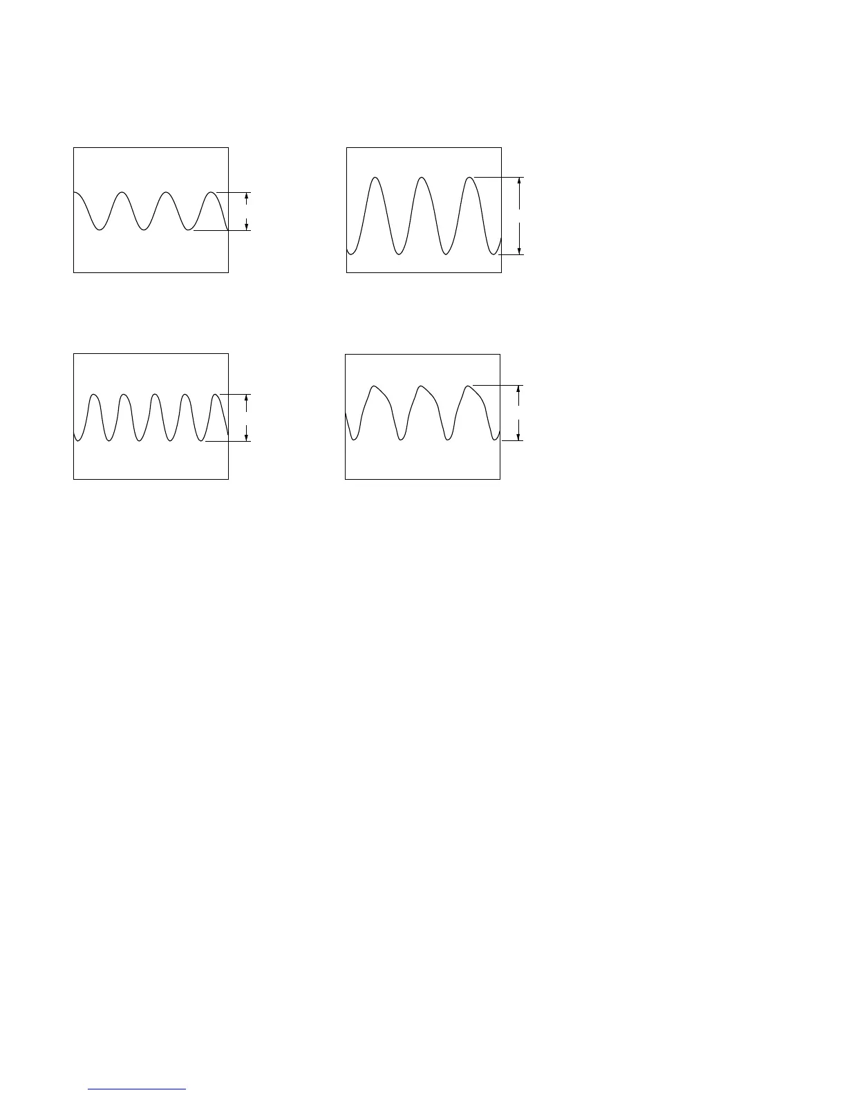
• Waveforms
1 IC401 !£ (XIN)
500 mV/DIV, 5µs/DIV
2 T301 (SECONDARY)
5 V/DIV, 200 ns/DIV
1.5 Vp-p
75.2 kHz
2 Vp-p
3.38 MHz
0.3 Vp-p
3.38 MHz
20.6 Vp-p
2.53 MHz
3 Q307 (COLLECTOR)
500 mV/DIV, 100 ns/DIV
4 Q307 (BASE)
100 mV/DIV, 100 ns/DIV
 Loading...