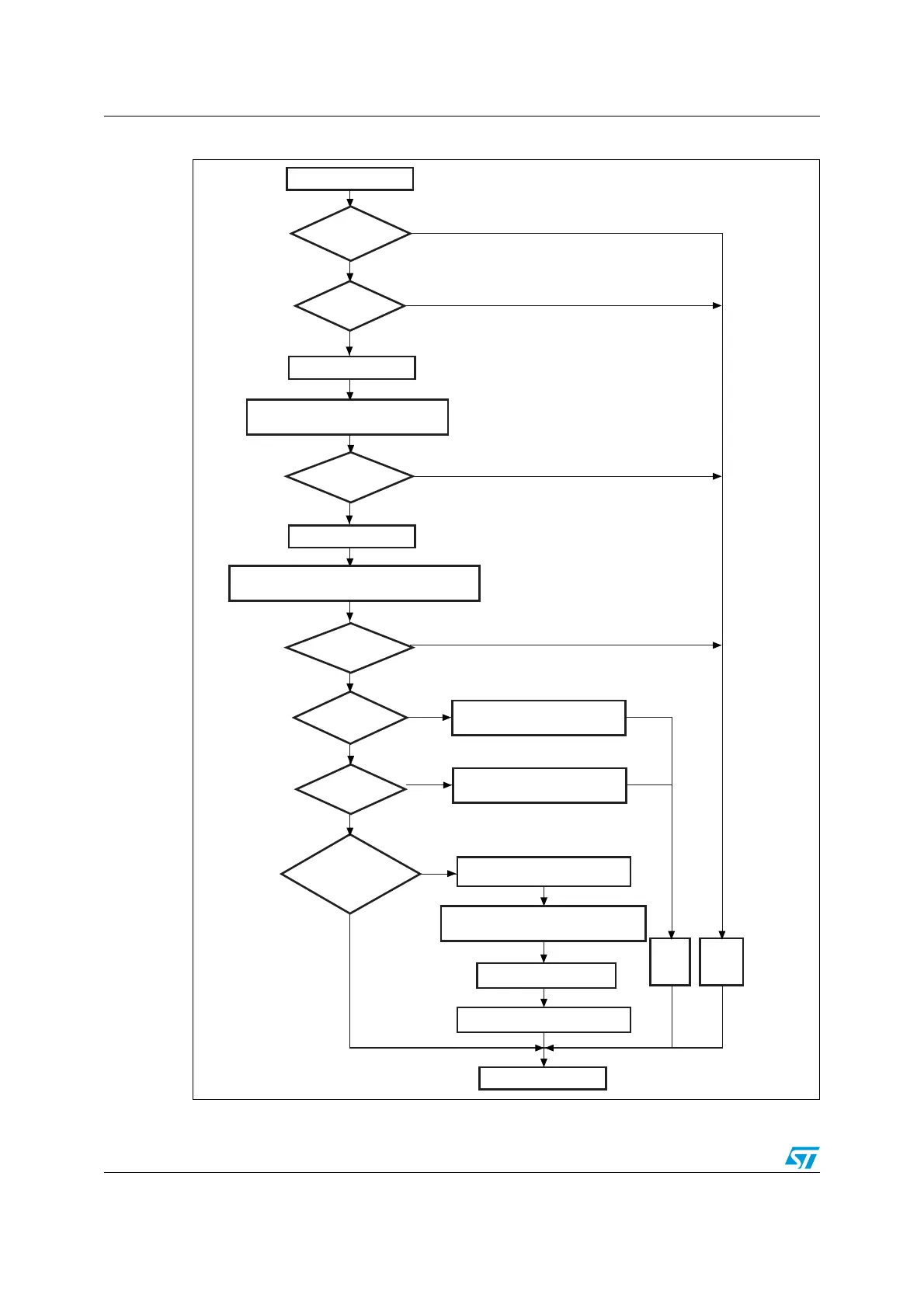
Figure 14. Write Memory command: device side
1. WM = Write Memory.
ROP inactive?
Receive the start address (4 bytes) &
checksum
Flash memory
address?
No
Ye s
ai14642b
Start WM
(1)
Receive the number of bytes to be written
(1 byte), the data (N + 1 bytes) & the checksum
Checksum OK?
No
Ye s
Received byte =
0x31+0xCE?
Send ACK byte
Send ACK byte
Write the received data to Flash
memory from the start address
Send
ACK
byte
End of WM
(1)
No
Ye s
No
Ye s
Checksum OK?
No
Ye s
RAM address?
Write the received data to RAM
from the start address
Ye s
Ye s
Option
byte address?
& address =
0x1FFF F800?
Write the received data to
Option byte area from start address
Ye s
Ye s
Write the Keys for Option byte
area access
Generate system reset
Send
NACK
byte
Send ACK byte

 Loading...


