Chapter 2: Installation
2-23
JLAN2
3
JSTBY
JCOM1
R625
MH7
MH1
MH5
41
FAN1
41
FAN2
4
1
FAN3
41
FAN4
41
FANA
JVR6
3
JVR5
1
3
JVR4
1
3
JVR3
1
3
JPB1
1
3
JPG1
1
JPL1
1
JPL2
JVR1
1
3
JVR2
1 3
JWD1
1
3
JPUSB1
1
JPME_RCV1
3
JPBIOS_RCV1
1
3
DP3
A
C
JI2C1
JI2C2
1
JOH1
1
JCF1
JL1
3-SGPIO2
1
2
7
8
3-SGPIO1
1
2
7
8
T-SGPIO1
2
7
8
T-SGPIO2
1
2
7
8
DIMM_C1
JUSB2
4
PCIX1
PCIX2
PCIX3
JPW1
1
12
24
JBT1
JPI2C1
1
5
SP1
+
PCIE6
PCIE5
PCIE4
X_BT1
JPW2
UID_LED
A
C
UID_SW
1
2
JTPM1
1
2
19
20
SAS4
SAS5 SAS6
SAS7 I-SATA2I-SATA3
I-SATA4
I-SATA5
JKBMS1
+
U8
JWF1
1
3
JTAG1
JD1
1
7
JF1
1
2
19
20
JVGA
JIPMB1
I-SATA1
I-SATA0
MAC CODE
MAC CODE
REV:1.01
Tested to Comply
With FCC Standards
FOR HOME OR OFFICE USE
DESIGNED IN USA
SAS CODE
JCOM2
1
5
6
9
JUSB45
2
7
10
JUSB67
1
2
7
JUSB89
1
2
7
10
JRK1
Pin3:PCH_DYN_SKU
Pin2:Ground
OFF:NORMAL
ON:ME IN FORCE UPDATA MODE
I-Button Header 1
Pin1:RAID_KEY_PCH
OFF:NORMAL
ON:RECOVER BIOS
UID
TPM/PORT80
JIPMB1
P1-DIMM4A
P1-DIMM4B
P1-DIMM3A
P1-DIMM3B
P1-DIMM2A
P1-DIMM2B
P1-DIMM1B
P1-DIMM1A
I-SATA5
I-SATA4
I-SATA3 I-SATA2
I-SATA1
I-SATA0
2-3 ENable
Power
Flash
KB/MOUSE
X9SRi
JPUSB1:USB Wake Up
1-2 Disable
PWRI2C
JF1
RST
ON
PWR
PWR
FF
FAIL
HDD
NIC
1
2
NIC
OH
LED
NMI
PWR
X
PWR LED
SPEAKER
1-3:
4-7:
JD1:
2-3:NMI
JWD1:Watch Dog
1-2:RST
LAN1
LAN2
JPL1/2: LAN
2-3 Disable
1-2 Enable
FAN4
VGA
COM1
USB0/1
INTRUSION
CHASSIS
OFF: SLAVE
ON: MASTER
JCF1:Compact Flash
Compact
SAS1/SAS3
SAS0/SAS2
3-SGPIO23-SGPIO1
Connect to IPMI
USB2
USB8/9
USB4/5
USB6/7
2-3 Disable
JPB: BMC
1-2 Enable
JSTBY : Wake on Lan
COM2
1-2 Enable
2-3 Disable
JPG1: VGA
OFF:DISABLE
ON: ENABLE
I2C Bus for PCI slot
JI2C1/JI2C2
SLOT4 PCI-E 3.0 X8 (IN X16)
SLOT5 PCI-E 2.0 X4 (IN X16)
SLOT6 PCI-E 3.0 X16
SLOT3 PCI-X 133/100MHZ
SLOT1 PCI-X 133/100MHZ
SLOT2 PCI-X 133/100MHZ
CLOSE 1st
OPEN 1st
JPW2
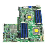
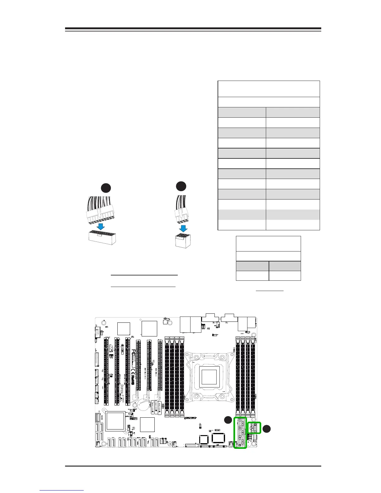
2-6 Connecting Cables & Optional Devices
This section provides brief descriptions and pin-out denitions for onboard headers
and connectors. Be sure to use the correct cable for each header or connector.
A. 24-Pin ATX Main PWR
B. 8-Pin Processor PWR
A
B
ATX Power 24-pin Connector
Pin Denitions (JPW1)
Pin# Denition Pin # Denition
13 +3.3V 1 +3.3V
14 -12V 2 +3.3V
15 Ground 3 Ground
16 PS_ON 4 +5V
17 Ground 5 Ground
18 Ground 6 +5V
19 Ground 7 Ground
20 -5V 8 PWR_OK
21 +5V 9 5VSB
22 +5V 10 +12V
23 +5V 11 +12V
24 Ground 12 +3.3V
(Required)
12V 8-pin Power Connec-
tor Pin Denitions
Pins Denition
1 through 4 Ground
5 through 8 +12V
ATX Main PWR (JPW1) & CPU PWR
Connectors (JPW2)
The 24-pin main power connector
(JPW1) is used to provide power to
the motherboard. The 8-pin CPU PWR
connector (JPW2) is also required for
the processor. These power connectors
meet the SSI EPS 12V specication. See
the table on the right for pin denitions.
8-Pin Processor PWR
A
B
24-Pin Main PWR
 Loading...