TM8100 Mobile Radio Service Manual Diagnosis of Faults on Main Board 189
May 2004 © Tait Electronics Limited
Tas k 3 —
Modulation or Noise
on VCO Tuning
Voltages
Noise or modulation can result in the frequency synthesizer providing a
tuning voltage that is approximately correct on average, but without
locking. Rectify the fault as follows:
1. Remove R570 [at 5M4/5F11] and R566 [at 5L4/5F10], which
provide a modulation path to the VCO(s) (see Figure 9.9).
2. Use the CCTM command 72 again to determine if the fault has
been removed. If it has, the CODEC and audio circuitry requires
investigation; go to Subsection 9.7. If the fault has not been
removed, replace R570 and R566, and go to Step 3.
3. The PLL is probably receiving insufficient RF power from the
VCO(s). Check for faults in the circuitry of the VCO(s) and
related buffer amplifier(s). If a fault is found, repair it, confirm the
removal of the fault, and return to Subsection 8.1. If the repair
failed or the fault could not be found, return to Subsection 8.1
and replace the complete main-board assembly.
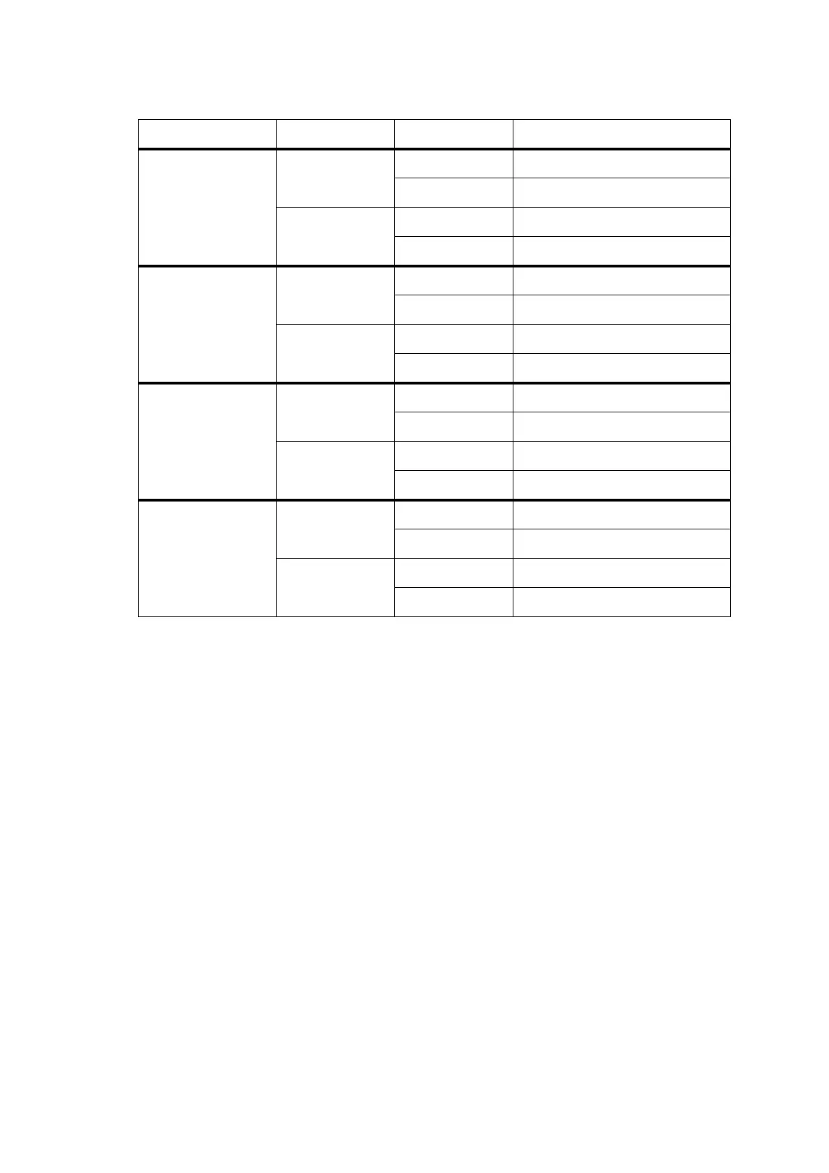
Table 9.2 Nominal VCO tuning voltages
Frequency band Mode Frequency Nominal VCO tuning voltage
B1 Receive Lowest 3 to 4 V
Highest 7 to 8 V
Transmit Lowest 5.5 to 6.5 V
Highest 9.5 to 10.5 V
D1 Receive Lowest 2.5 to 3.5
Highest 7.5 to 8.5
Transmit Lowest 5 to 6
Highest 10 to 11
H5 Receive Lowest 3 to 4 V
Highest 11 to 12 V
Transmit Lowest 3 to 4 V
Highest 10.5 to 11.5 V
H6 Receive Lowest 2.5 to 3.5 V
Highest 11 to 12.5 V
Transmit Lowest 2 to 3 V
Highest 10 to 11 V
 Loading...