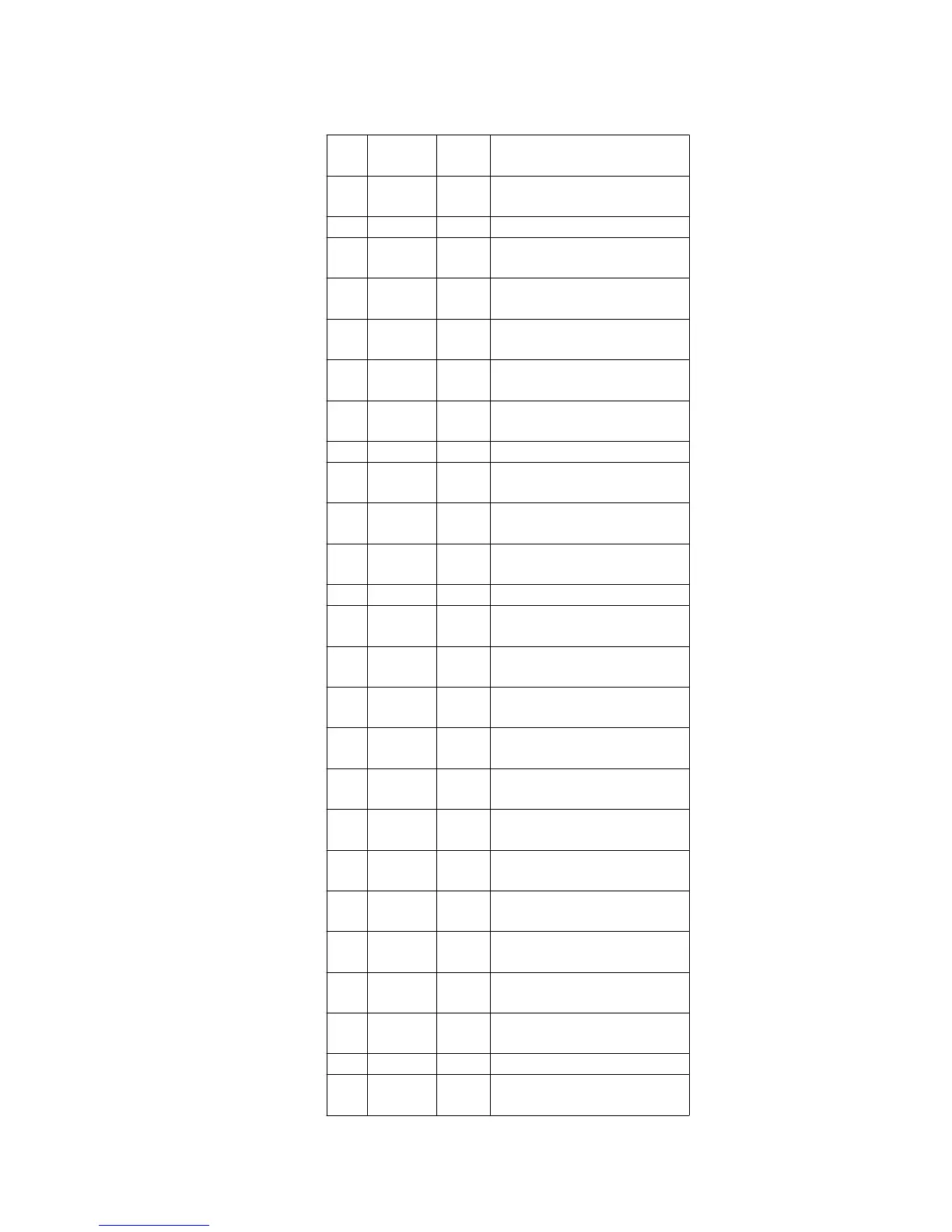
Pin
No.
Mark I/O
Division
Function
1 CENVD — D signal det. capacitor
connection terminal
2 LDO O Laser amp output terminal
3 APCPD I Photo diode light quantity
det. input terminal
4 LD IN I Laser amp reverse input
terminal
5 APC REF I APC amp criterion voltage
input terminal
6 TEMP IN I Temperature sensor amp
input terminal
7 TEMP O Temperature sensor amp
output terminal
8 ADIP O ADIP signal output terminal
9 TOFS I Tracking error offset
adjustment terminal
10 TBAL I Tracking ballance
adjustment terminal
11 TE O Tracking error signal
output terminal
12 CRS IN I Track cross input terminal
13 TGAIN I Tracking gain adjustment
input terminal
14 LNP O Lens position signal
output terminal
15 AB GAIN I APP compensation signal
gain adjustment terminal
16 FE O Focus error signal output
terminal
17 AS GAIN I AS gain adjustment
terminal
18 FBAL I Focus ballance adjustment
terminal
19 AS/
MON3T
O AS/3TMON signal output
terminal
20 CEA I 3T envelope det. capacitor
connection terminal
21 BDO/
TRCRS
O BDO/Track cross signal
output terminal
22 CBD O O BDO detection capacitor
connection terminal
23 OFT O O Off track detection signal
output terminal
24 GND — GND terminal
25 OFT IN I Off track detection signal
input terminal
38