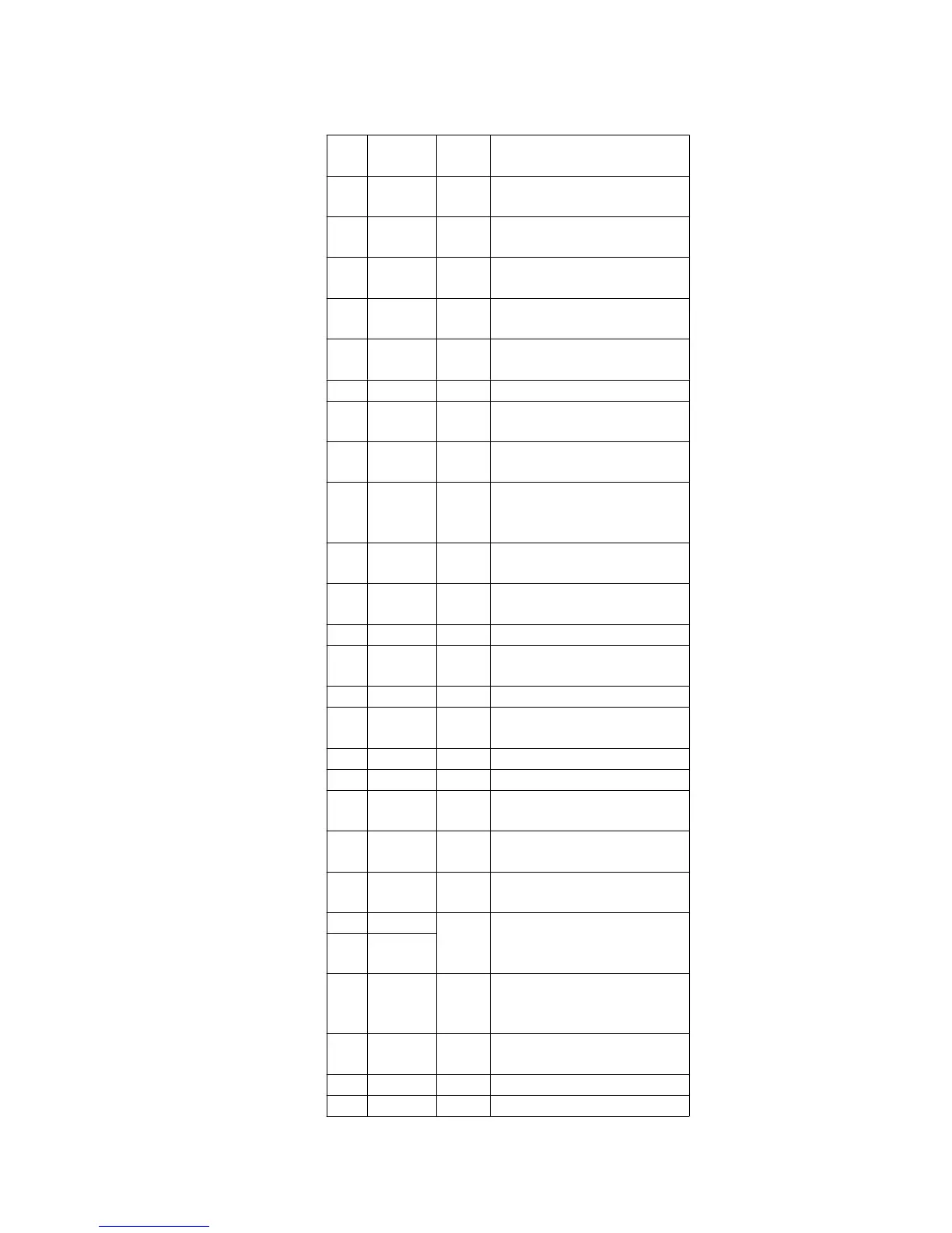
Pin
No.
Mark I/O
Division
Function
1 P97 O VR control clock output
terminal
2 P96 O VR control data output
terminal
3 P95 O VR control STB output
terminal
4 P94 O Digital in 1/2 select signal
output terminal (“H”: in 1)
5 P93 I Not used, connected to
GND
6 P92 I Chip select input terminal
7 P91 O Request signal output
terminal
8 P90 O Reset signal output
terminal
9 CNVSS — Flash write signal voltage
(Connected to GND
through resistor)
10 P87 O Power on/off control signal
output terminal
11 P86 — Not used, connected to
GND
12 RESET I Reset signal input terminal
13 XOUT O Clock ceramic oscillator
output terminal (f=10MHz)
14 VSS — GND terminal
15 XIN I Clock ceramic oscillator
output terminal (f=10MHz)
16 VCC I Power supply terminal
17 P85 I AC detect terminal
18 P84 I Remote control data input
terminal
19 P83 I Unit load switch signal
input terminal
20 P82 O Audio mute signal output
terminal
21 P81 O Play LED drive signal
output terminal (“L”: LED
on)
22 P80
23 P77 I Not used, connected to
power supply through
resistor
24 P76 O Communication clock
output terminal
25 P75 I Data input terminal
26 P74 O Data output terminal
51