16VORTEK Doc.# VT5 OM 050499, Rel. 2.1
4.3 Offset Adjustment
The tag on the transmitter enclosure may have two separate values for frequency; Full
scale Hz and Span Hz. If this is the case, the transmitter was factory calibrated with an
offset. To set the offset, follow the set up procedure in 4.2 first. Next turn the offset
potentiometer (see figure 5) counter clockwise all the way. Now input the span fre-
quency to the transmitter, and adjust the span potentiometer until the output is 20.0 mA.
Next input the Full Scale frequency. The mA output will go up. Turn the offset potentiom-
eter clockwise until the output is 20.0 mA again. The adjustment is complete.
4.4 Calibration Check
1. Follow the setup instructions shown in section 4.2 (in the “Set full scale” section) of
the manual.
2. The check should include 3 points: 1/2 full scale frequency, 3/4 full scale frequency,
and the full scale frequency. Input these frequencies using the method in “Set full
scale”. The transmitter output will be 12 mA, 16 mA, and 20 mA respectively.
3. If the calibration does not match the above, recalibration will be required. The cali-
bration should match the entire range of operation. If it agrees at the maximum fre-
quency but not in the center, there may be a problem with the way the unit is configured.
It is likely that jumper JP 1 is not set properly. It should be in the down position if full
scale frequency is greater than 600 Hz.
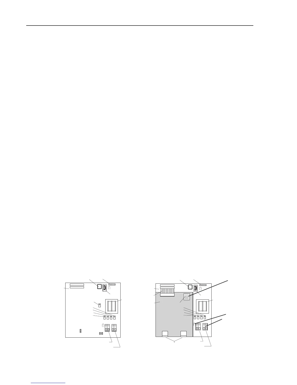
4.5 Wave form check with an oscilloscope
Voltage Input - See figure 5, below. Set up the oscilloscope to read wave forms clearly
on the screen. To check the power input, set the scope to read 24VAC. Touch the
negative test lead to either screw in the power wire connector (A), and the positive lead
to the other screw. The screen should read 60Hz.
Connect the negative lead to the test point 1 (TP1) (B) on the mother board. Connect
the positive lead to one of the exposed metal jumpers (C) on the amplifier board. A
clean, square wave should appear, and the numerical frequency value should not
bounce more the 20% for a good signal. Check each of the thin metal jumpers and read
the values. The average frequencies of the jumpers should be fairly close in value. If
there are two amplifier boards on top of the mother board, the top amplifier board must
be removed.
POWER
DISPLAY
OUTPUT
SETUP
DIP
PROGRAM
MODULE
PROBE INPUTS
SIGNAL
JUMPERS
SUMMI NG
BOARD
MOTHER
BOARD
RIBBON
CABLE
ZERO
SPAN
OFFSET
DISPLAY
TP5
TRANSFORMER
TP1
ZERO
SPAN
OFFSET
DISPLAY
DISPLAY
OUTPUT
SETUP
DIP
PROGRAM
MODULE
SIGNAL
POWER
JP1 (3-pin)
THRESHOLD POT.
MOTHER
BOARD
JP2 JP3
TRANSFORMER
TP5
TP1
Figure 5 - Vortek Mother Board, (left); VorTek mother board showing summing board (right).
A
B
C
Chapter 4 Calibration and Maintenance
 Loading...