SECTION 3
CIRCUIT DESCRIPTION
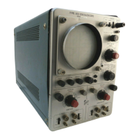
Type 503
Introduction
NOTE
This section of the manual contains detailed circuit
description and analysis. To follow the theory of circuit
operation as presented, refer to the Schematic Diagram
section in this manual.
VERTICAL AMPLIFIER
General Description
The Vertical Amplifier consists of two identical input cir
cuits, two matching step attenuators, a two-stage Input
Amplifier, and a DC-coupled push-pull Output Amplifier.
The Input Amplifier first stage is made up of two hybrid
feedback pairs which drive a DC-coupled push-pull Out
put Amplifier. Vertical sensitivity is controlled by step
attenuation at the inputs, and by changing the gain of the
Input Amplifiers. Variable attenuation is accomplished by
degeneration in the cathode circuit of the Output Amplifier.
Input Circuits
The separate input connectors permit the Input Ampli
fier to be operated either single ended or as a differential
amplifier. For single-ended operation, either input connec
tor can be used, while the other input connector is ground
ed. Convenient input switches at each connector allow DC
or AC coupling, or grounding of the inputs. The lower fre
quency limit of the amplifier with AC coupling is approxi
mately 7.5 Hz (0.75 Hz with 10X probe).
In the 1 mV/CM to .2VOLTS/CM positions of the SEN
SITIVITY switch, the signal is applied without attenuation
to the grid circuit (or circuits) of the Input Amplifier; changes
in sensitivity are accomplished by changing the Input Ampli
fier gain (i.e., switching R408). In the .5 VOLTS/CM to 2
VOLTS/CM positions of the SENSITIVITY switch, a X10
attenuator network is inserted in addition to gain changing.
In the 5 VOLTS/CM to 20 VOLTS/CM switch positions, a
X100 attenuation network is inserted in addition to gain
changing.
The attenuating networks are composed of resistance and
capacitance dividers. For DC and low-frequency signals,
the attenuators act as resistance dividers, because the re
actance of the capacitors at low frequencies is so high
that their effect on the input signal can be neglected; at
the higher frequencies, however, the lower capacitive re
actance becomes effective. Near the upper frequency range
of the amplifier, the reactance of the capacitors becomes
so low that the attenuators are primarily capacitive dividers.
In addition to providing the correct degree of attenua
tion, the resistance values are chosen so that the input
resistance is a constant 1 megohm shunted by 47 pF, regard
less of the setting of the SENSITIVITY switch.
Input Amplifier
The operation of the Input Amplifier will be described
using the amplifier with single-ended input.
At Instrument Serial Number 6997, each ha lf o f
the dual-triode input stage was replaced by a
nuvistor-type triode, to improve the am plifier drift
characteristics. Since circuit number designations
were changed at the same time, reference to each
half of the input stage w ill be made by associa
tion with the input to which it is connected; i.e.,
+ INPUT grid or — INPUT grid.
The Input Amplifier consists of two high gain, feedback
amplifiers, V434, Q454 and V444, Q464. Due to feedback
the gain is one from V434 grid to the junction of R408,
R419 and R436. The gain from V444 grid to the junction of
R408, R419 and R446 is also one.
Note that Q454 and Q464 emitters are returned to a
common point. The voltage at the common point is held
virtually constant because as the current in Q454 is de
creased the current in Q464 is increased a like amount. This
fixed potential is reflected to V434 and V444 plate loads
through Q454 and Q464 emitter-base junctions. If V434
and V444 plate loads see a constant voltage the current
must be constant. Therefore, the current in V434 and V444
is held constant (changes in Q454 and Q464 base current
will appear in V434 and V444 but is small enough to be
ignored).
Assume that the + INPUT is grounded ( + INPUT AC-DC-
GND switch is in the GND position) and a positive going
signal is applied to the —INPUT. Since the +INPUT is
grounded and the gain from V444 grid to the junction of
R408, R419 and R446 is one, the junction will not move
when the positive going signal on V434 causes the junction
of R408, R419 and R436 to move positive. A current is forced
to flow through R408 and R419 but since the current in V434
and V444 cannot change, the current must come from Q464
and flow through R467, to R457 and Q454. The current
change through R467 and R457 will force Q464 collector to
move negative and Q454 collector to move positive. The
ratio of the signal out (measured between Q454 and Q464
collectors) to signal in of the amplifier may be expressed
as:
A —- 1 +
R457 + R467
R*
R457
+ R438
, where
R* = R408 in parallel with R419. R438 appears in the equa
tion because as R* becomes large (.05, .1 and ,2 V ranges)
R438 will contribute some current in R457, causing an
. , , . R457
increase in gain by the ratio - .
R438
The second stage of the Input Amplifier is provided with
a positive feedback path network from the collector of each
side to the base of the other. This positive feedback
increases the amplifier gain (open loop) to infinity, thus
allowing the feedback components R457, R467 and R408
3-1