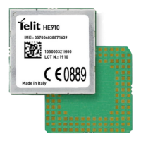
HE910 Hardware User Guide
1VV0300925 Rev. 32 Page 96 of 111 2019-11-25
It is not recommended to place via or micro-via not covered by solder resist in an area of
0,3 mm around the pads unless it carries the same signal of the pad itself (see following
figure).
Figure 15-6 PCB pads
Holes in pad are allowed only for blind holes and not for through holes.
Recommendations for PCB pad surfaces:
Electro-less Ni /
Immersion Au
good solder ability protection,
high shear force values
The PCB must be able to resist the higher temperatures which are occurring at the lead-
free process. This issue should be discussed with the PCB-supplier. Generally, the
wettability of tin-lead solder paste on the described surface plating is better compared to
lead-free solder paste.
It is not necessary to panel the application’s PCB, however in that case it is suggested to
use milled contours and predrilled board breakouts; scoring or v-cut solutions are not
recommended.