)~-------
~
945424-9701
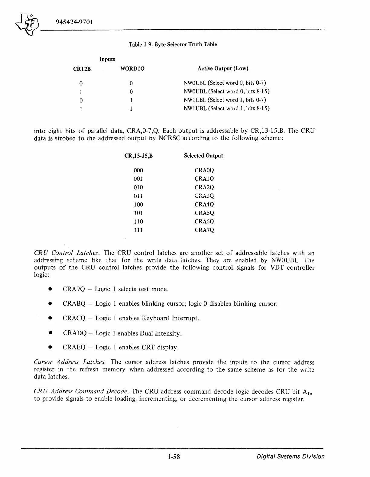
Table 1-9. Byte Selector Truth Table
CR12B
0
1
0
Inputs
WORDlQ
0
0
Active
Output
(Low)
NWOLBL
(Select word 0, bits 0-7)
NWOUBL
(Select word 0, bits 8-15)
NWI
LBL (Select word 1, bits 0-7)
NWl UBL (Select word 1, bits 8-15)
into
eight bits
of
parallel
data,
CRA,0-7 ,Q. Each
output
is
addressable
by
CR, 13-15.B. The
CRU
data
is
strobed
to
the
addressed
output
by
NCRSC according
to
the
following scheme:
CR,13-15,B
Selected
Output
000
CRAOQ
001
CRAlQ
010
CRA2Q
(\
1 1
en
.i"'lrt.
V.11
1'.fi.)
\,/_
100
CRA4Q
101
CRASQ
110
CRA6Q
111
CRA7Q
CR U Control Latches. The CRU
control
latches are
another
set
of
addressable latches with an
addressing scheme like
that
for
the
write
data
latches. They are enabled by NWOUBL. The
outputs
of
the
CRU
control
latches provide
the
following
control
signals for VDT
controller
logic:
•
CRA9Q
- Logic 1 selects
test
mode.
• CRABQ - Logic 1 enables blinking cursor; logic 0 disables blinking cursor.
• CRACQ - Logic 1 enables Keyboard
Interrupt.
• CRADQ - Logic 1 enables Dual
Intensity.
• CRAEQ - Logic 1 enables
CRT
display.
Cursor Address Latches. The cursor address latches provide
the
inputs
to
the cursor address
register in
the
refresh
memory
when addressed according
to
the
same scheme
as
for
the
write
data
latches.
CRU
Address
Command
Decode. The CRU address
command
decode logic decodes CRU bit A
16
to
provide signals
to
enable loading, incrementing,
or
decrementing the cursor address register.
1-58
Digital
Systems Division