ACTV
BANK
ROW
DDR2CLKOUT
DDR2CLKOUT
DCE0
DSDCKE
DSDRAS
DSDWE
DSDDQM[3:0]
DSDCAS
DBA[2:0]
DEA[13:0]
Peripheral Architecture
www.ti.com
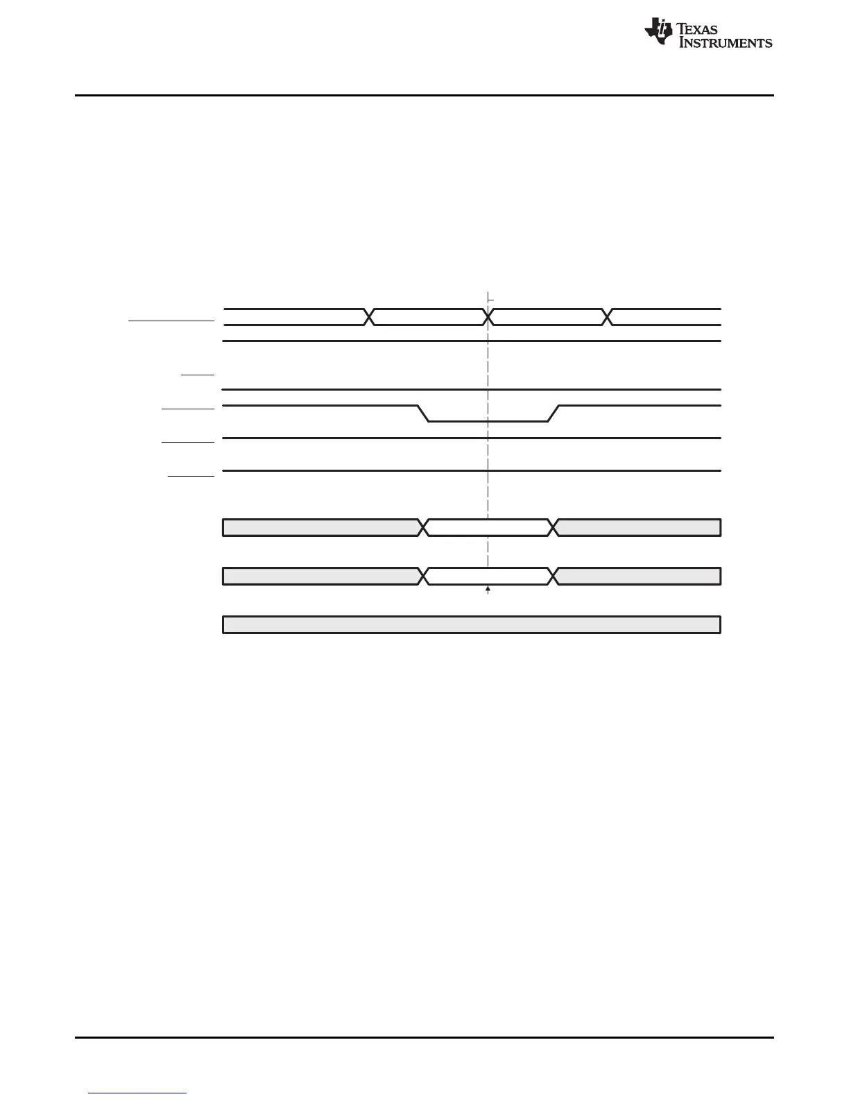
2.4.3 Activation (ACTV)
The DDR2 memory controller automatically issues the activate (ACTV) command before a read or write to
a closed row of memory. The ACTV command opens a row of memory, allowing future accesses (reads or
writes) with minimum latency. The value of DBA[2:0] selects the bank and the value of A[12:0] selects the
row. When the DDR2 memory controller issues an ACTV command, a delay of t
RCD
is incurred before a
read or write command is issued. Figure 5 shows an example of an ACTV command. Reads or writes to
the currently active row and bank of memory can achieve much higher throughput than reads or writes to
random areas because every time a new row is accessed, the ACTV command must be issued and a
delay of t
RCD
incurred.
Figure 5. ACTV Command
16
C6455/C6454 DDR2 Memory Controller SPRU970G– December 2005– Revised June 2011
Submit Documentation Feedback
Copyright © 2005–2011, Texas Instruments Incorporated

 Loading...