Col. 0 Col. 1 Col. 2 Col. 3 Col. 4 Col. M−1 Col. M
Row 0, bank 0
Row 0, bank 1
Row 0, bank 2
Row 0, bank P
Row 1, bank 1
Row 1, bank 0
Row 1, bank 2
Row 1, bank P
Row N, bank 2
Row N, bank 1
Row N, bank 0
Row N, bank P
www.ti.com
Peripheral Architecture
Ending the current access is not a condition that forces the active DDR2 SDRAM row/page to be closed.
The DDR2 memory controller leaves the active row open until it becomes necessary to close it. This
decreases the deactivate-reactivate overhead.
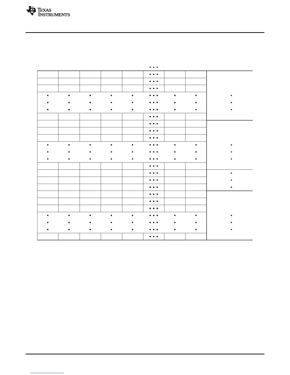
Figure 13. Logical Address-to-DDR2 SDRAM Address Map
A M is number of columns (as determined by PAGESIZE) minus 1, P is number of banks (as determined by IBANK)
minus 1, and N is number of rows (as determined by both PAGESIZE and IBANK) minus 1.
23
SPRU970G– December 2005– Revised June 2011 C6455/C6454 DDR2 Memory Controller
Submit Documentation Feedback
Copyright © 2005–2011, Texas Instruments Incorporated

 Loading...