www.ti.com
List of Figures
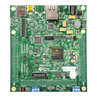
1-1. TMS570LC43 HDK Board Block Diagram................................................................................ 6
2-1. TMS570LC43 HDK Board, Interfaces Top Side ......................................................................... 8
2-2. Connectors on TMS570LC43 HDK........................................................................................ 9
2-3. CAN Bus Termination...................................................................................................... 11
2-4. J2, J3 CAN Bus Interface (Screw Terminal)............................................................................ 11
2-5. J19, 60 Pin MIPI ETM Header............................................................................................ 12
2-6. +12 V Input Jack ........................................................................................................... 14
2-7. J9, J10, and J11 on HDK ................................................................................................. 15
2-8. DIP Switch Settings........................................................................................................ 18
List of Tables
1-1. TMS570LC43 Memory Map ................................................................................................ 7
1-2. Power Test Points ........................................................................................................... 7
2-1. Connectors on HDK Board ................................................................................................. 9
2-2. 20-Pin ARM JTAG Header................................................................................................ 10
2-3. J1, Ethernet Interface...................................................................................................... 10
2-4. J19, MIPI Connector Signal Mapping.................................................................................... 12
2-5. J19, MIPI Connector Signal Mapping.................................................................................... 13
2-6. J7, XDS100V2 USB JTAG Interface..................................................................................... 14
2-7. Expansion Connector P1 (J9, Left, BottomView) ...................................................................... 15
2-8. Expansion Connector P2 (J10, Right, BottomView) ................................................................... 16
2-9. Expansion Connector P3 (J11, Bottom One, TopView)............................................................... 17
2-10. Demo LEDs ................................................................................................................. 18
2-11. Other LEDs as Indicator................................................................................................... 18
2-12. S2 DIP Switch Functions.................................................................................................. 19
2-13. Jumpers ..................................................................................................................... 19
3
SPNU597–May 2014 List of Figures
Submit Documentation Feedback
Copyright © 2014, Texas Instruments Incorporated