Contents
Preface ........................................................................................................................................ 4
1 Introduction......................................................................................................................... 5
1.1 Scope of Document ......................................................................................................... 5
1.2 TMS570LC43 HERCULES Development Kit (HDK) Features......................................................... 5
1.3 HDK Board Block Diagram ................................................................................................. 6
1.4 TMS570LC43 HDK Contents .............................................................................................. 6
1.5 Basic Operation .............................................................................................................. 7
1.6 Memory Map ................................................................................................................. 7
1.7 Power Supply................................................................................................................. 7
2 Physical Description............................................................................................................. 8
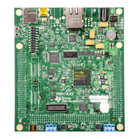
2.1 Board Layout ................................................................................................................. 8
2.2 Connectors ................................................................................................................... 9
2.2.1 20-Pin ARM JTAG Header....................................................................................... 10
2.2.2 Ethernet Interface ................................................................................................. 10
2.2.3 CAN Interface...................................................................................................... 10
2.2.4 J19, MIPI ETM Connector........................................................................................ 12
2.2.5 J7, XDS100V2 USB JTAG Interface............................................................................ 14
2.2.6 P1, +5 V to +12 V Input .......................................................................................... 14
2.2.7 SCI Interface....................................................................................................... 14
2.2.8 Daughter Card Interface.......................................................................................... 14
2.3 LEDs ......................................................................................................................... 18
2.4 S2 DIP Switch .............................................................................................................. 18
2.5 Jumpers ..................................................................................................................... 19
2.6 S4, Power On Reset Switch .............................................................................................. 19
2.7 S3, System Reset Switch ................................................................................................. 19
A Operation Notices............................................................................................................... 20
2
Contents SPNU597–May 2014
Submit Documentation Feedback
Copyright © 2014, Texas Instruments Incorporated