EasyManua.ls Logo

Texas Instruments TMS320F28069 - User Manual

Texas Instruments TMS320F28069
177 pages
Print Icon
To Next Page IconTo Next Page
Loading...
Product
Folder
Sample &
Buy
Technical
Documents
Tools &
Software
Support &
Community
An IMPORTANT NOTICE at the end of this data sheet addresses availability, warranty, changes, use in safety-critical applications,
intellectual property matters and other important disclaimers. PRODUCTION DATA.
TMS320F28069
,
TMS320F28068
,
TMS320F28067
,
TMS320F28066
TMS320F28065, TMS320F28064, TMS320F28063, TMS320F28062
SPRS698F –NOVEMBER 2010–REVISED MARCH 2016
TMS320F2806x Piccolo™ Microcontrollers
1 Device Overview
1
1.1 Features
1
• High-Efficiency 32-Bit CPU (TMS320C28x)
– 90 MHz (11.11-ns Cycle Time)
– 16 × 16 and 32 × 32 Multiply and Accumulate
(MAC) Operations
– 16 × 16 Dual MAC
– Harvard Bus Architecture
– Atomic Operations
– Fast Interrupt Response and Processing
– Unified Memory Programming Model
– Code-Efficient (in C/C++ and Assembly)
• Floating-Point Unit (FPU)
– Native Single-Precision Floating-Point
Operations
• Programmable Control Law Accelerator (CLA)
– 32-Bit Floating-Point Math Accelerator
– Executes Code Independently of the Main CPU
• Viterbi, Complex Math, CRC Unit (VCU)
– Extends C28x Instruction Set to Support
Complex Multiply, Viterbi Operations, and Cyclic
Redundency Check (CRC)
• Embedded Memory
– Up to 256KB of Flash
– Up to 100KB of RAM
– 2KB of One-Time Programmable (OTP) ROM
• 6-Channel Direct Memory Access (DMA)
• Low Device and System Cost
– Single 3.3-V Supply
– No Power Sequencing Requirement
– Integrated Power-on Reset and Brown-out
Reset
– Low-Power Operating Modes
– No Analog Support Pin
• Endianness: Little Endian
• JTAG Boundary Scan Support
– IEEE Standard 1149.1-1990 Standard Test
Access Port and Boundary Scan Architecture
• Clocking
– Two Internal Zero-Pin Oscillators
– On-Chip Crystal Oscillator/External Clock Input
– Watchdog Timer Module
– Missing Clock Detection Circuitry
• Peripheral Interrupt Expansion (PIE) Block That
Supports All Peripheral Interrupts
• Three 32-Bit CPU Timers
• Advanced Control Peripherals
• Up to 8 Enhanced Pulse-Width Modulator (ePWM)
Modules
– 16 PWM Channels Total (8 HRPWM-Capable)
– Independent 16-Bit Timer in Each Module
• Three Input Enhanced Capture (eCAP) Modules
• Up to 4 High-Resolution Capture (HRCAP)
Modules
• Up to 2 Enhanced Quadrature Encoder Pulse
(eQEP) Modules
• 12-Bit Analog-to-Digital Converter (ADC), Dual
Sample-and-Hold (S/H)
– Up to 3.46 MSPS
– Up to 16 Channels
• On-Chip Temperature Sensor
• 128-Bit Security Key and Lock
– Protects Secure Memory Blocks
– Prevents Reverse-Engineering of Firmware
• Serial Port Peripherals
– Two Serial Communications Interface (SCI)
[UART] Modules
– Two Serial Peripheral Interface (SPI) Modules
– One Inter-Integrated-Circuit (I
2
C) Bus
– One Multichannel Buffered Serial Port (McBSP)
Bus
– One Enhanced Controller Area Network (eCAN)
– Universal Serial Bus (USB) 2.0
(see Device Comparison Table for Availability)
• Full-Speed Device Mode
• Full-Speed or Low-Speed Host Mode
• Up to 54 Individually Programmable, Multiplexed
General-Purpose Input/Output (GPIO) Pins With
Input Filtering
• Advanced Emulation Features
– Analysis and Breakpoint Functions
– Real-Time Debug Through Hardware
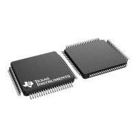
• 2806x Packages
– 80-Pin PFP and 100-Pin PZP PowerPAD™
Thermally Enhanced Thin Quad Flatpacks
(HTQFPs)
– 80-Pin PN and 100-Pin PZ Low-Profile Quad
Flatpacks (LQFPs)
Question and Answer IconNeed help?

Do you have a question about the Texas Instruments TMS320F28069 and is the answer not in the manual?

Summary

1 Device Overview

1.1 Features

Lists the key features and capabilities of the TMS320F2806x microcontroller family.

1.2 Applications

1.3 Description

1.4 Functional Block Diagram

1.5 System Device Diagram

2 Revision History

3 Device Comparison

4 Terminal Configuration and Functions

4.1 Pin Diagrams

Illustrates the pin configurations for different package types of the microcontroller.

4.2 Signal Descriptions

5 Specifications

5.1 Absolute Maximum Ratings

Defines the absolute maximum ratings for supply voltage, input voltage, and other parameters.

5.2 ESD Ratings for TMS320 F2806 xU

Specifies the Electrostatic Discharge (ESD) ratings for the TMS320F2806xU devices.

5.3 ESD Ratings for TMS320 F2806 x, TMS320 F2806 xM, and TMS320 F2806 xF

Details the ESD ratings for TMS320F2806x, TMS320F2806xM, and TMS320F2806xF devices.

5.4 Recommended Operating Conditions

5.5 Electrical Characteristics

5.6 Power Consumption Summary

5.7 Thermal Resistance Characteristics

5.8 Thermal Design Considerations

5.9 Emulator Connection Without Signal Buffering for the MCU

5.10 Parameter Information

5.10.1 Timing Parameter Symbology

Defines the symbology used for various timing parameters according to JEDEC standards.

5.10.2 General Notes on Timing Parameters

Provides important general notes regarding timing parameters and signal transitions.

5.11 Test Load Circuit

5.12 Power Sequencing

5.13 Clock Specifications

5.13.1 Device Clock Table

Lists the cycle times and frequencies for various clocks available on the 2806x MCUs.

5.13.2 Clock Requirements and Characteristics

Details the requirements and characteristics for on-chip and external clock sources.

5.14 Flash Timing

5.14 Flash Timing

Details the flash and OTP endurance ratings for different temperature materials.

6 Detailed Description

6.1 Overview

General overview of the device's architecture and peripherals.

6.1.3 Viterbi, Complex Math, CRC Unit (VCU)

6.1.4 Memory Bus (Harvard Bus Architecture)

6.1.5 Peripheral Bus

6.1.6 Real-Time JTAG and Analysis

6.1.7 Flash

6.1.8 M0, M1 SARAMs

6.1.9 L4 SARAM, and L0, L1, L2, L3, L5, L6, L7, and L8 DPSARAMs

6.1.10 Boot ROM

6.1.11 Security

6.1.12 Peripheral Interrupt Expansion (PIE) Block

6.1.13 External Interrupts (XINT1-XINT3)

6.1.14 Internal Zero Pin Oscillators, Oscillator, and PLL

6.1.15 Watchdog

6.1.16 Peripheral Clocking

6.1.17 Low-power Modes

6.1.18 Peripheral Frames 0, 1, 2, 3 (PFn)

6.1.19 General-Purpose Input;Output (GPIO) Multiplexer

6.1.20 32-Bit CPU-Timers (0, 1, 2)

6.1.21 Control Peripherals

6.1.22 Serial Port Peripherals

6.2 Memory Maps

6.3 Register Maps

6.4 Device Emulation Registers

6.5 VREG, BOR, POR

6.5.1 On-chip VREG

Details the on-chip voltage regulator (VREG) functionality and its usage.

6.5.2 On-chip Power-On Reset (POR) and Brown-Out Reset (BOR) Circuit

Explains the on-chip POR and BOR circuits for device reset during power-up and operation.

6.6 System Control

6.6.1 Internal Zero Pin Oscillators

Describes the two independent internal zero-pin oscillators and their configuration.

6.6.2 Crystal Oscillator Option

Covers the crystal oscillator option, including pin connections and specifications.

6.6.3 PLL-Based Clock Module

Details the PLL-based clock module, its ratio control, and operating frequency settings.

6.6.4 USB and HRCAP PLL Module (PLL2)

6.6.5 Loss of Input Clock (NMI Watchdog Function)

6.6.6 CPU-Watchdog Module

6.7 Low-power Modes Block

6.8 Interrupts

6.8.1 External Interrupts

Details external interrupt registers and their configuration.

6.9 Peripherals

6.9.1 Control Law Accelerator (CLA) Overview

Provides an overview of the Control Law Accelerator, its architecture, and features.

6.9.2 Analog Block

6.9.2.1 Analog-to-Digital Converter (ADC)

Details the features and functions of the 12-bit ADC, including conversion modes and triggers.

6.9.2.2 ADC MUX

6.9.2.3 Comparator Block

6.9.2.3.1 On-Chip Comparator;DAC Electrical Data;Timing

Provides electrical data and timing for the on-chip comparator and DAC.

6.9.4 Serial Peripheral Interface (SPI) Module

6.9.4.1 SPI Master Mode Electrical Data;Timing

Details the SPI master mode timing requirements and switching characteristics.

6.9.4.2 SPI Slave Mode External Timing (Clock Phase = 0)

Provides SPI slave mode timing for clock phase 0, including requirements and waveforms.

6.9.5 Serial Communications Interface (SCI) Module

6.9.6 Multichannel Buffered Serial Port (McBSP) Module

6.9.6.1 McBSP Transmit and Receive Timing

Details McBSP transmit and receive timing requirements.

6.9.6.1.2 McBSP as SPI Master or Slave Timing

Provides McBSP timing requirements when acting as SPI master or slave.

6.9.7 Enhanced Controller Area Network (eCAN) Module

6.9.8 Inter-Integrated Circuit (I2 C)

6.9.8.1 I2 C Electrical Data;Timing

Provides electrical data and timing specifications for the I2C module.

6.9.9 Enhanced Pulse Width Modulator (ePWM) Modules (ePWM1-ePWM8)

6.9.9.1 ePWM Electrical Data;Timing

Details ePWM timing requirements and switching characteristics.

6.9.9.2 Trip-Zone Input Timing

Provides timing requirements for Trip-Zone inputs.

6.9.10 High-Resolution PWM (HRPWM)

6.9.10.1 HRPWM Electrical Data;Timing

Details the high-resolution PWM switching characteristics.

6.9.11 Enhanced Capture Module (eCAP1)

6.9.12 High-Resolution Capture Modules (HRCAP1-HRCAP4)

6.9.13 Enhanced Quadrature Encoder Modules (eQEP1, eQEP2)

6.9.13.1 eQEP Electrical Data;Timing

Provides eQEP timing requirements and switching characteristics.

6.9.14 JTAG Port

6.9.15 General-Purpose Input;Output (GPIO) MUX

6.9.15.1 GPIO Output Timing

Details the timing characteristics for general-purpose output signals.

6.9.15.1.2 GPIO Input Timing

Provides timing requirements for general-purpose input signals and qualification modes.

6.9.15.1.3 Sampling Window Width for Input Signals

6.9.15.1.4 Low-Power Mode Wakeup Timing

6.9.16 Universal Serial Bus (USB)

6.9.16.1 USB Electrical Data;Timing

Provides USB electrical data and timing requirements for input and output ports.

7 Applications, Implementation, and Layout

7.1 TI Design or Reference Design

Lists TI Designs Reference Design Library resources for system design evaluation.

7.1.1 Digitally Controlled Non-Isolated DC;DC Buck Converter Reference Design

Describes a reference design for a digitally controlled DC/DC buck converter.

7.1.2 672 W Highly Integrated Reference Design for Automotive Bidirectional 48 V-12 V Converter

Details a reference design for a 48V-12V bidirectional converter for automotive applications.

7.1.3 System-on-Module for Power Line Communication Reference Design

Describes a SOM for PLC in the CENELEC frequency band, supporting industry standards.

7.1.4 G3 Power Line Communications Data Concentrator on BeagleBone Black Platform

Presents a PLC Data Concentrator design for evaluating G3-PLC on a Beagle Bone Black.

7.1.5 Texas Instruments Power Line Communication Developers Kit - V3

Introduces the TI PLC Developer's Kit for evaluating PLC technology in industrial applications.

7.1.6 DC Power Line Communication (PLC) Reference Design

7.2 Development Tools

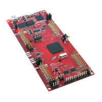
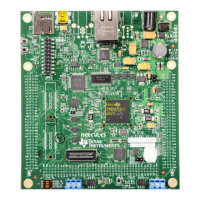
7.2.1 F28069 Piccolo controlCARD

Introduces the F28069 Piccolo controlCARD for initial software development and system prototyping.

7.2.2 F28069 Piccolo controlSTICK

Highlights the F28069 Piccolo controlSTICK for quick evaluation of microcontroller capabilities.

7.2.3 F28069 Piccolo Experimenter Kit

Describes the F28069 Piccolo Experimenter Kit for device exploration and testing.

7.3 Software Tools

7.3.1 controlSUITE Software Suite

Introduces controlSUITE, a software suite for C2000 microcontrollers to minimize development time.

7.3.2 Code Composer Studio (CCS) Integrated Development Environment (IDE)

Describes Code Composer Studio (CCS), an IDE for developing and debugging embedded applications.

7.3.3 Pin Mux Tool

Explains the Pin Mux Utility for configuring pin multiplexing and I/O cell characteristics.

7.4 Training

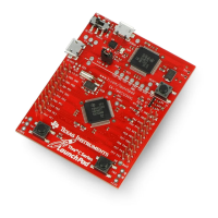
7.4.1 InstaSPIN-FOC LaunchPad and BoosterPack

Provides information on the C2000 InstaSPIN-FOC Motor Control LaunchPad Kit.

7.4.2 C2000 Architecture and Peripherals

Overviews the C2000 family architecture and its offered peripherals.

7.4.3 Piccolo Control Law Accelerator (CLA) Technical Overview

Offers a technical overview of the Piccolo CLA, describing its floating-point math capabilities.

8 Device and Documentation Support

8.1 Device Support

Details TI's development tools for C28x generation MCUs, including software and hardware tools.

8.1.1 Development Support

Details TI's development tools for C28x generation MCUs, including software and hardware tools.

8.1.1.1 Getting Started

Provides key links for getting started with C2000 Real-time Control MCUs, motor drive, digital power, and tools.

8.1.2 Device and Development Support Tool Nomenclature

Explains the prefixes and evolutionary stages used in TI device and tool nomenclature.

8.2 Documentation Support

8.2.1 Receiving Notification of Document Updates

Guides users on how to receive notifications for documentation updates via ti.com.

8.3 Related Links

8.4 Community Resources

8.5 Trademarks

8.6 Electrostatic Discharge Caution

8.7 Glossary

9 Mechanical Packaging and Orderable Information

9.1 Packaging Information

States that subsequent pages provide mechanical packaging and orderable information for designated devices.

Texas Instruments TMS320F28069 Specifications

General IconGeneral
Architecture32-bit
Core Speed90 MHz
Clock Speed90 MHz
Program Memory Size128 KB
RAM Size20 KB
ADC12-bit
ADC Channels16
Operating Voltage3.3 V
PackageLQFP-100
CPU TypeTMS320C28x
Communication InterfacesCAN, I2C, SPI, UART

Related product manuals