21
TMS320F28069
,
TMS320F28068
,
TMS320F28067
,
TMS320F28066
TMS320F28065, TMS320F28064, TMS320F28063, TMS320F28062
www.ti.com
SPRS698F –NOVEMBER 2010–REVISED MARCH 2016
Submit Documentation Feedback
Product Folder Links: TMS320F28069 TMS320F28068 TMS320F28067 TMS320F28066 TMS320F28065
TMS320F28064 TMS320F28063 TMS320F28062
SpecificationsCopyright © 2010–2016, Texas Instruments Incorporated
(1) I
DDIO
current is dependent on the electrical loading on the I/O pins.
(2) In order to realize the I
DDA
currents shown for IDLE, STANDBY, and HALT, clock to the ADC module must be turned off explicitly by
writing to the PCLKCR0 register.
(3) The TYP numbers are applicable over room temperature and nominal voltage.
(4) The following is done in a loop:
• Data is continuously transmitted out of SPI-A, SPI-B, SCI-A, eCAN-A, McBSP-A, and I
2
C ports.
• The hardware multiplier is exercised.
• Watchdog is reset.
• ADC is performing continuous conversion.
• COMP1 and COMP2 are continuously switching voltages.
• GPIO17 is toggled.
(5) CLA is continuously performing polynomial calculations.
(6) For F2806x devices that do not have CLA, subtract the I
DD
current number for CLA (see Table 5-2) from the I
DD
(VREG disabled)/I
DDIO
(VREG enabled) current numbers shown in Table 5-1 for operational mode.
(7) If a quartz crystal or ceramic resonator is used as the clock source, the HALT mode shuts down the on-chip crystal oscillator.
(8) To realize the I
DD
number shown for HALT mode, the following must be done:
• PLL2 must be shut down by clearing bit 2 of the PLLCTL register.
• A value of 0x00FF must be written to address 0x6822.
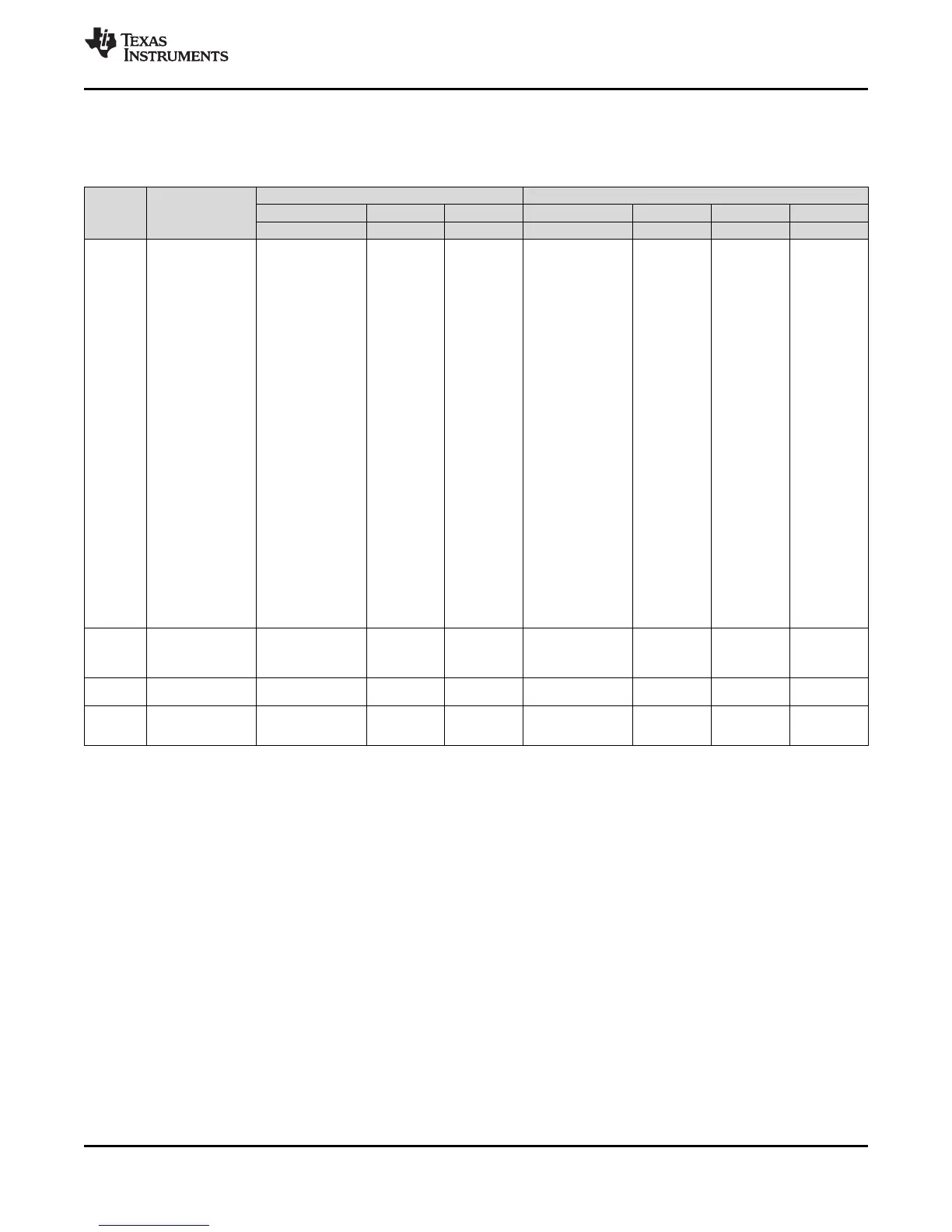
5.6 Power Consumption Summary
Table 5-1. TMS320F2806x Current Consumption at 90-MHz SYSCLKOUT
MODE TEST CONDITIONS
VREG ENABLED VREG DISABLED
I
DDIO
(1)
I
DDA
(2)
I
DD3VFL
I
DD
I
DDIO
(1)
I
DDA
(2)
I
DD3VFL
TYP
(3)
MAX TYP
(3)
MAX TYP
(3)
MAX TYP
(3)
MAX TYP
(3)
MAX TYP
(3)
MAX TYP
(3)
MAX
Operational
(Flash)
The following peripheral
clocks are enabled:
• ePWM1, ePWM2,
ePWM3, ePWM4,
ePWM5, ePWM6,
ePWM7, ePWM8
• eCAP1, eCAP2,
eCAP3
• eQEP1, eQEP2
• eCAN
• CLA
• HRPWM
• SCI-A, SCI-B
• SPI-A, SPI-B
• ADC
• I
2
C
• COMP1, COMP2,
COMP3
• CPU-TIMER0,
CPU-TIMER1,
CPU-TIMER2
• McBSP
• USB
All PWM pins are toggled
at 90 kHz.
All I/O pins are left
unconnected.
(4) (5)
Code is running out of
flash with 3 wait-states.
XCLKOUT is turned off.
185 mA
(6)
245 mA
(6)
16 mA 22 mA 35 mA 40 mA 165 mA
(6)
220 mA
(6)
15 mA 20 mA 16 mA 22 mA 35 mA 40 mA
IDLE
Flash is powered down.
XCLKOUT is turned off.
All peripheral clocks are
turned off.
22 mA 27 mA 15 µA 25 µA 5 µA 10 µA 21 mA 26 mA 120 µA 400 µA 15 µA 25 µA 5 µA 10 µA
STANDBY
Flash is powered down.
Peripheral clocks are off.
9 mA 11 mA 15 µA 25 µA 5 µA 10 µA 8 mA 10 mA 120 µA 400 µA 15 µA 25 µA 5 µA 10 µA
HALT
Flash is powered down.
Peripheral clocks are off.
Input clock is disabled.
(7)
75 µA 15 µA 25 µA 5 µA 10 µA 25 µA
(8)
40 µA 15 µA 25 µA 5 µA 10 µA