10-bit
DAC
Analog
Comparators
CMP1-Out
CMP2-Out
CMP3-Out
Trip Zone
Temp
Sensor
ADC
(DMA-
accessible)
12-bit
3.46-MSPS
Dual
Sample-
and-
Hold
SOC-based
V
REF
CLA Core
90-MHz Floating-Point
(Accelerator)
(DMA-accessible)
10-bit
DAC
10-bit
DAC
A0
A2
A3
A4
A5
A6
A7
B0
B1
B2
B3
B4
B5
B6
B7
A1
6
eQEP 2´
HRCAP 4´
eCAP 3´
System
Vreg
Int-Osc-1
POR/BOR
Int-Osc-2
On-chip Osc
WD
PLL
CLKSEL
Timers 32-bit
Timer-0
Timer-1
Timer-2
GPIO
Control
COMMS
X1
X2
V
REFLO
V
REFHI
C28x
Core
(90-MHz)
FPU
VCU
Flash Memory
RAM
RAM
(Dual-Access)
eQEP
8
HRCAP
4
eCAP
3
4
8
2
2
6
PWM-1A
PWM-1B
PWM-2A
PWM-2B
PWM-3A
PWM-3B
PWM-4A
PWM-4B
PWM-5A
PWM-5B
PWM-6A
PWM-6B
PWM-7A
PWM-7B
PWM-8A
PWM-8B
TZ1
TZ2
TZ3
CMP1-out
CMP2-out
CMP3-out
PWM1
(DMA-accessible)
PWM5
(DMA-accessible)
PWM8
(DMA-accessible)
PWM7
(DMA-accessible)
PWM6
(DMA-accessible)
PWM4
(DMA-accessible)
PWM3
(DMA-accessible)
PWM2
(DMA-accessible)
UART 2´
SPI 2´
I C
2
CAN
McBSP
(DMA-accessible)
2
USB
(DMA-accessible)
4
TMS320F28069
,
TMS320F28068
,
TMS320F28067
,
TMS320F28066
TMS320F28065, TMS320F28064, TMS320F28063, TMS320F28062
SPRS698F –NOVEMBER 2010–REVISED MARCH 2016
www.ti.com
Submit Documentation Feedback
Product Folder Links: TMS320F28069 TMS320F28068 TMS320F28067 TMS320F28066 TMS320F28065
TMS320F28064 TMS320F28063 TMS320F28062
Device Overview Copyright © 2010–2016, Texas Instruments Incorporated
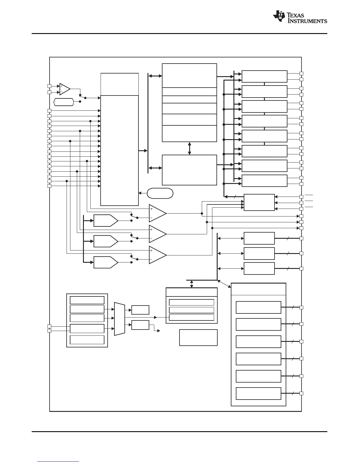
1.5 System Device Diagram
Figure 1-2. Peripheral Blocks